X-ray inspection is used to inspect the quality and reliability of products containing electronics by revealing hidden defects such as soldering issues, voids, misalignments, and component damage that may not be visible externally. By identifying potential problems early in the production process, X-ray inspection helps prevent failures, reduce rework costs, and enhance the overall performance and longevity of these products. This post demonstrates three inspection tools made possible using high resolution digital x-ray imaging..
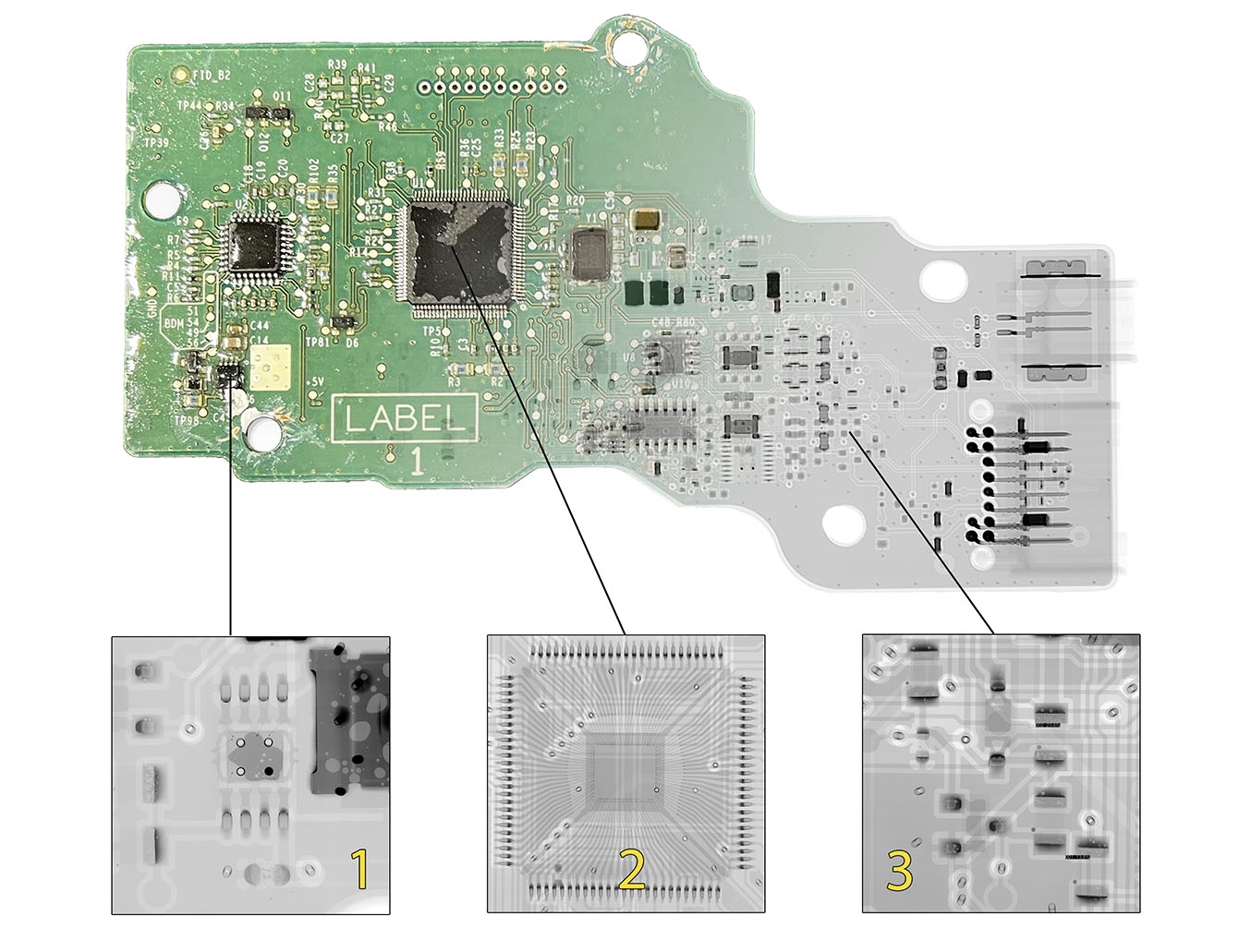
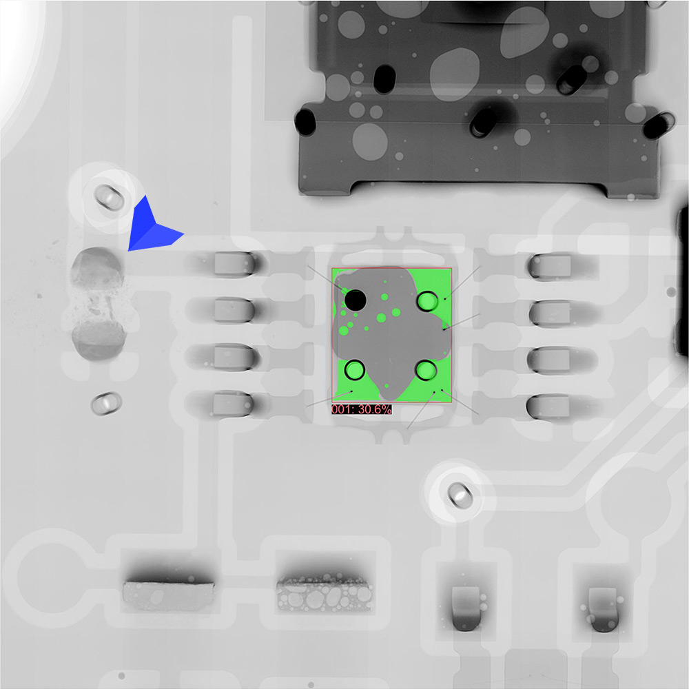
1. Solder Pad Fill
X-ray is used to ensure that the solder completely fills the pad to create a strong, conductive joint.
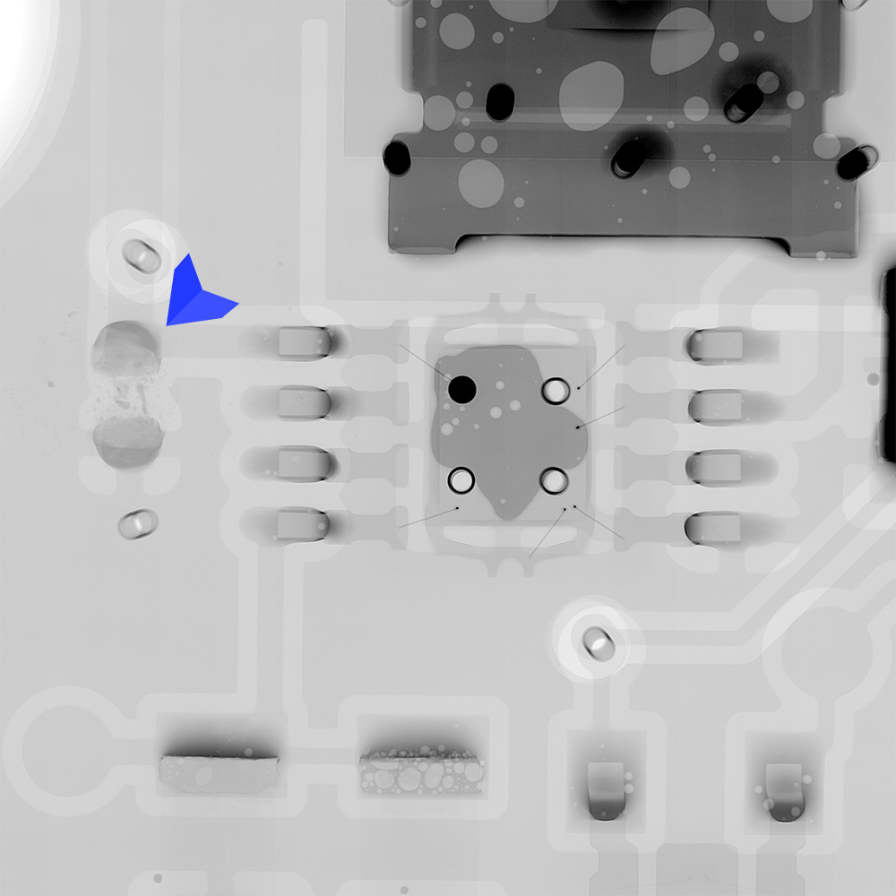
2. fpga wire sweep analysis
X-ray is used to examine the deformation of bonding wires within a microchip package which could potentially cause electrical shorts
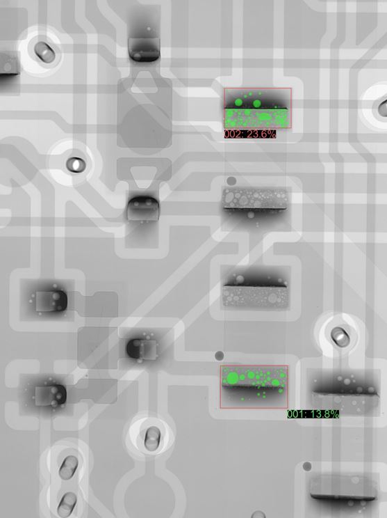
3. SOLDER JOINT POROSITY X-RAY INSPECTION
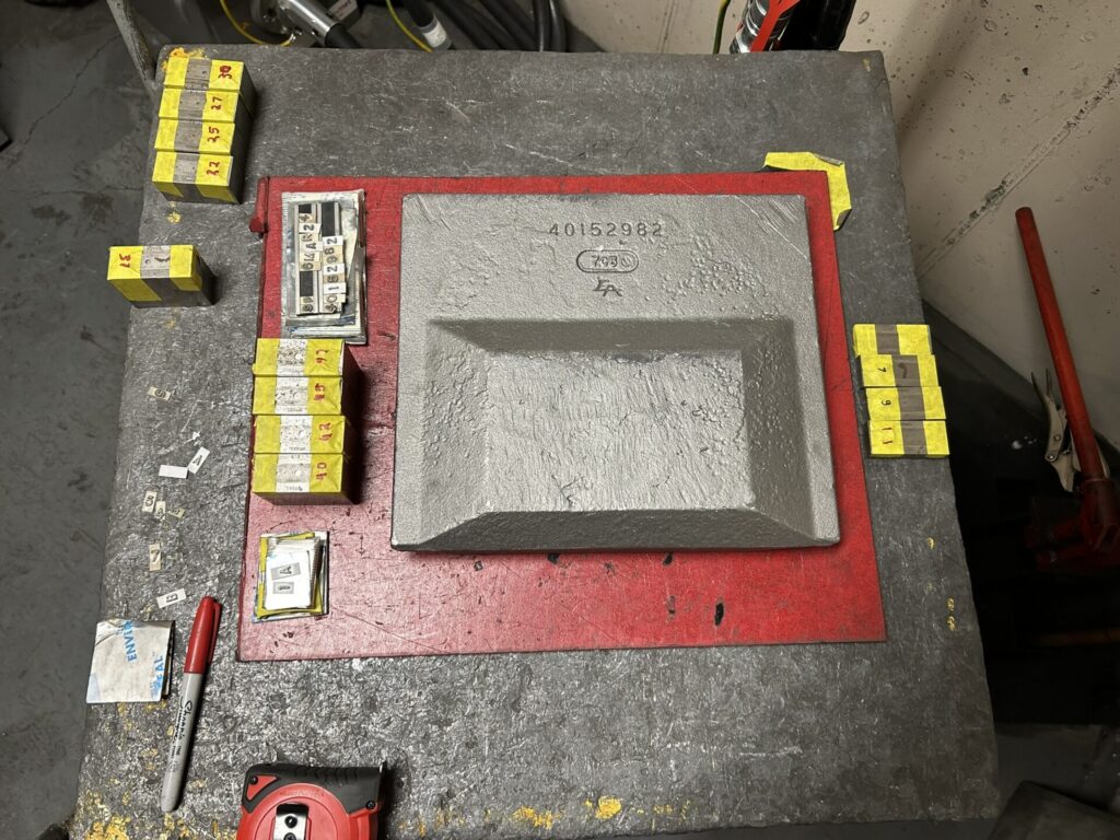
X-ray is used to detect small air pockets or voids within the solder joints of a printed circuit board. We follow custom quality standards provided by our clients to identify areas where process adjustments might be needed. For example, automotive porosity standards typically call for less than 20% porosity in any joint.
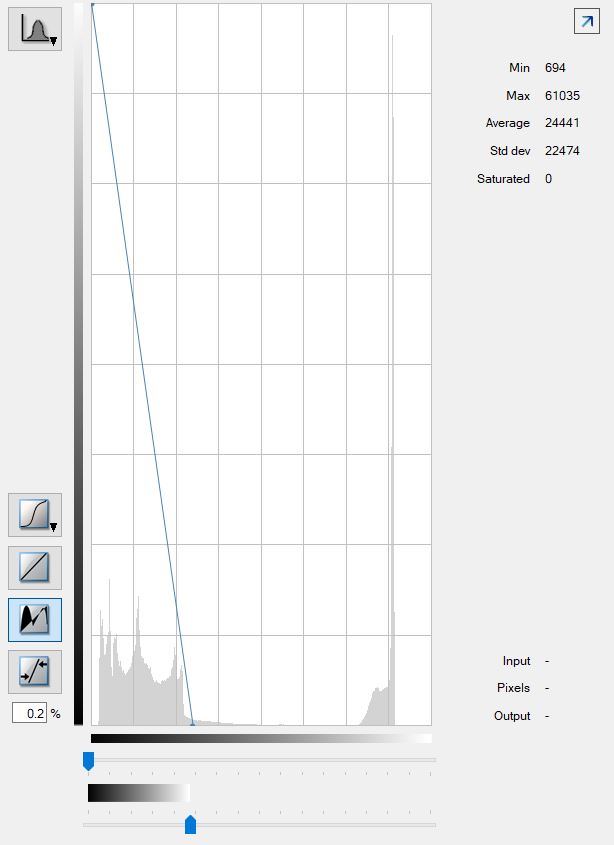
Radiographic Testing can be summarized as interpreting the differential absorption of X-rays. But X-rays are a band of electromagnetic radiation that cannot be detected with human senses (sight, smell, taste, etc.) so, how do we interpret them?
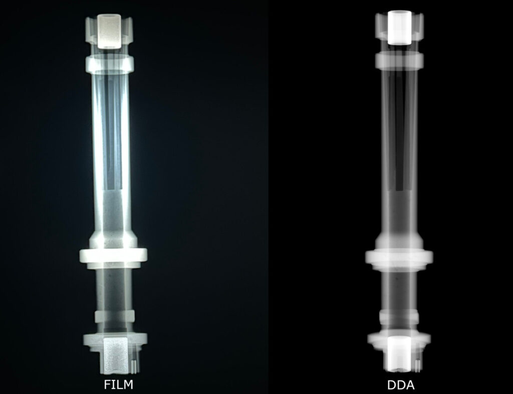
Traditionally this has been done using photographic film. The film has an emulsion layer made up of silver halide crystals. These tiny crystals are light sensitive and X-rays really are just a form of light so, the crystals get excited when exposed to an X-ray.
The X-rays get attenuated at varying rates based on material thicknesses and density. Less X-rays will reach the film (or crystals) when imaging a thick section of an object compared to a thin section. Similarly, less X-rays will reach the film when imaging a more dense part made of steel vs a less dense part made of aluminum. This differential absorption (difference in X-rays making their way to a silver halide crystal) creates a latent image on the film which can then be developed into a permanent photograph with chemical processing that separates the exposed crystals from the unexposed.
Reviewing a Film Radiograph
Film has been the standard medium for capturing radiographic images since it was first pioneered by Wilhelm Röntgen in 1895. In fact, it still has prolific use in the non-destructive testing industry today. However, these days there are other options which are becoming increasingly adopted.
Digital detector array (DDA) technology was introduced in the last few decades and is becoming increasingly popular as the technology gets better and becomes more affordable. Rather than silver halide crystals, these detectors use a matrix of photodiodes to measure the rate of X-ray absorption. And unlike film, there is no physical radiograph. Instead the image is viewed digitally on a computer.
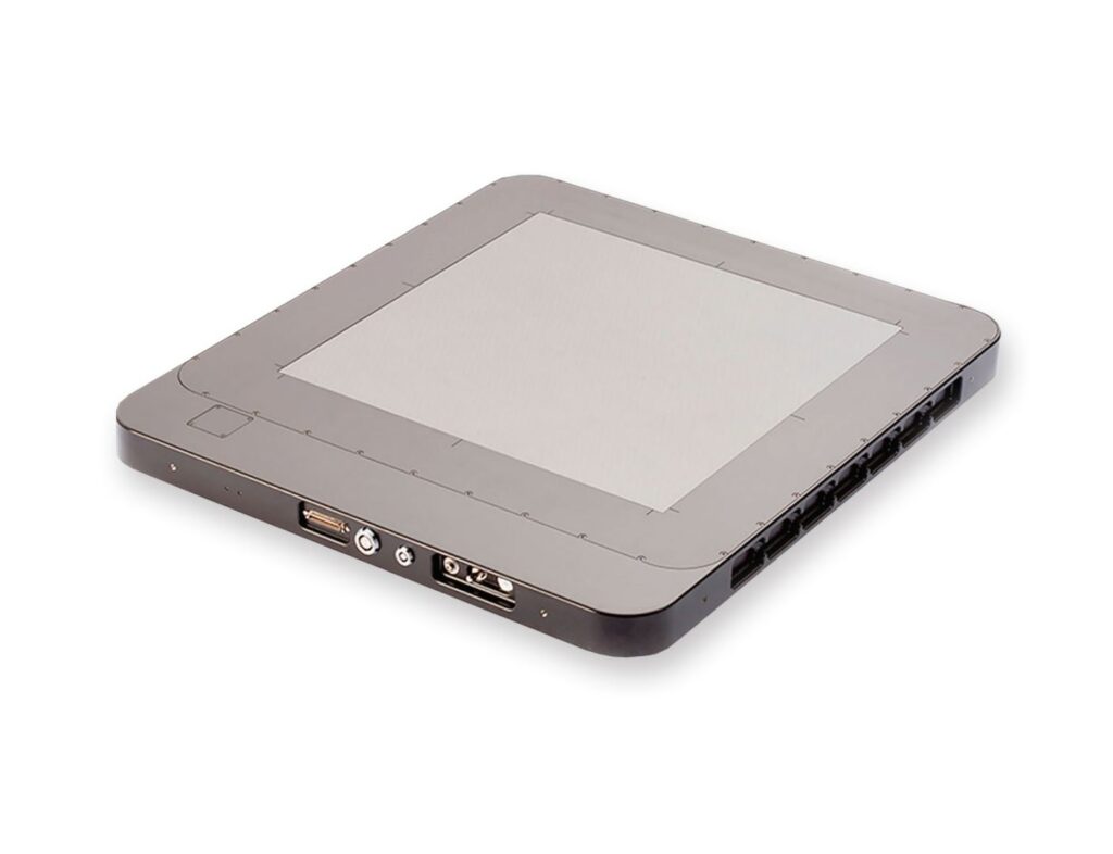
An example of a Digital Detector Array
Film Density & Digital Image Gray Scale
With film the optical density of the radiograph cannot be adjusted after the film has been developed. An optimal density range is targeted using specific exposure settings, film type, and developing time but there is a lot that can go wrong. If the area of interest on the developed film is too dark (or too light) the exposure must be reshot. It takes time and expensive materials to expose and develop a film radiograph. This all goes to waste if a reshoot is required.
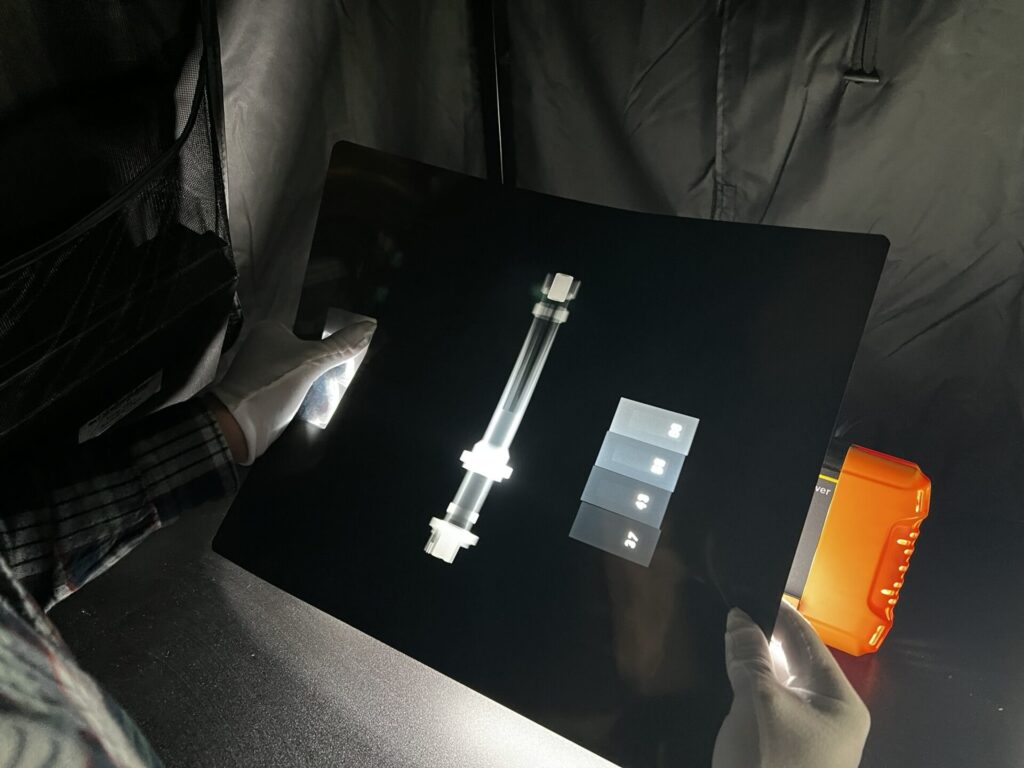
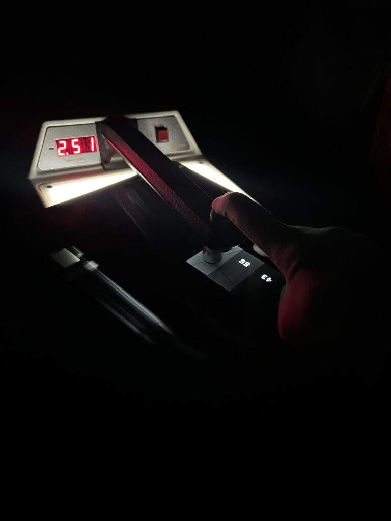
Using a densitometer to check optical density of a film radiograph
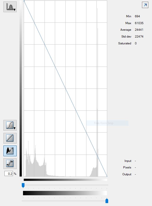
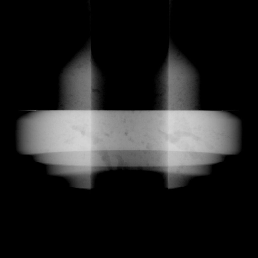
With digital imaging you get to see the results right away on your computer screen without a lengthy development time and smelly chemicals. Additionally, the brightness and contrast can be electronically adjusted which provides cushion for less than optimal exposure parameters. To put this into context, the human eye can distinguish about 500 shades of gray, but a digital radiograph taken with a 16 bit detector has 65,536 shades of gray. The 16 bit image has so much information that we cannot actually discern it all by just viewing the raw image alone. To make full use of these thousands of indistinguishable shades of gray we adjust ‘window/level’ (similar to brightness/contrast) to optimize the viewing window for a given area of interest.
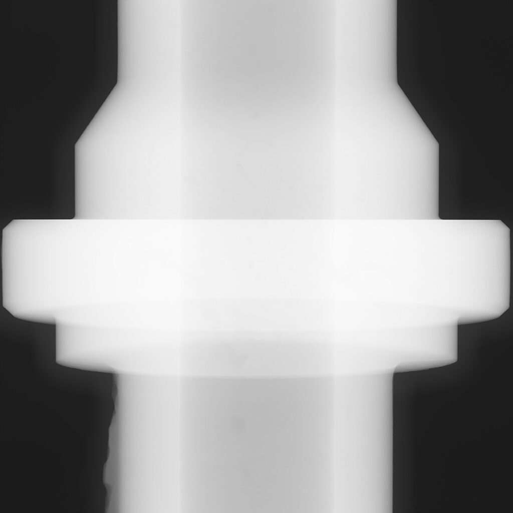
Digital image with a wide open window - defects hardly visible
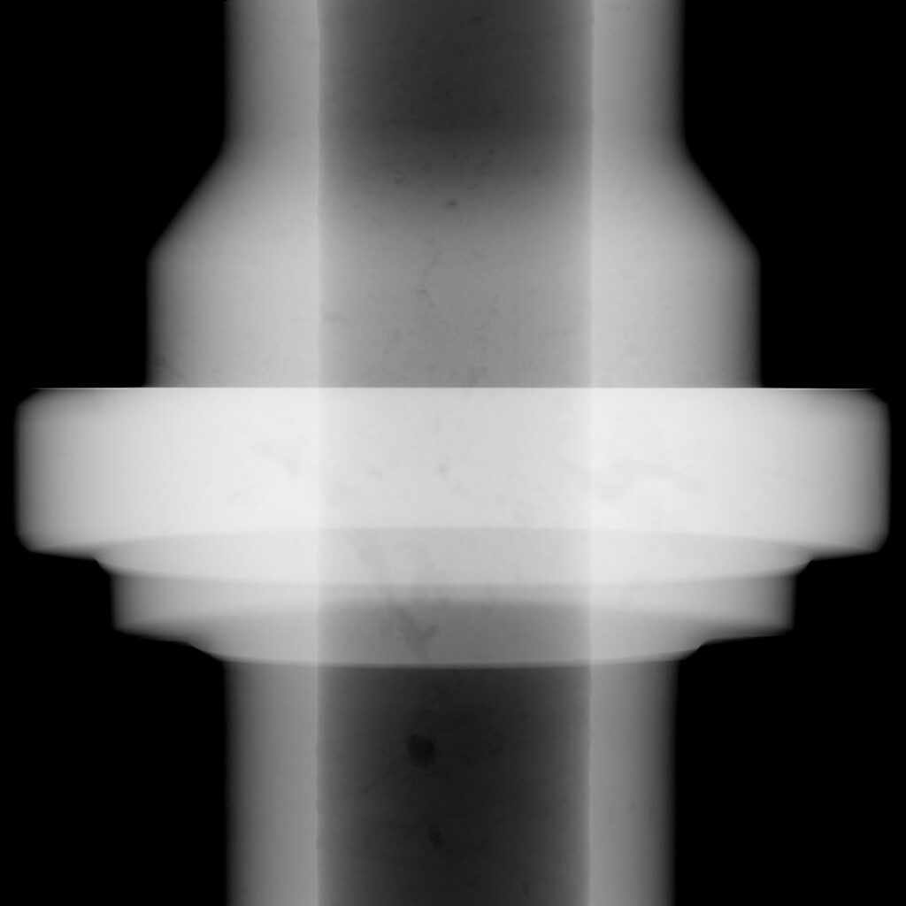
Same digital image with a tighter window - defects clear in the thin region, somewhat clear in the thick region
Same digital image with an even tighter window - defects in the thin region not within level range, but defects in the thick region more clear
Portability
One of the clear shortfalls of Digital Radiography is the need for a power source. This is not an issue in a lab environment but out in the field this means lugging around extension cables and computers. There are some battery operated DDAs out there but this does not fully remedy the power issue if operating for long periods of time or environments with extreme temperatures.
DDAs are also typically rigid and heavy. This makes them tough to set in place. If dropped the DDA could be damaged. Some manufacturers have begun to develop flexible DDAs to address this issue.
On the other hand Film Radiography is extremely pliable. It can be wrapped around a pipe. It can be cut down to size to fit into tight or oddly shaped areas. If combined with a gamma source of radiation, Film Radiography can be performed with no electrical hookups whatsoever.
Another good option for portability is Computed Radiography (CR) with photostimulable phosphor imaging plates. I can’t compare Film & DDA in the field without mentioning CR but that’s a different box of worms for another post. Just know CR can be thought of as a hybridization of Film Radiography and DDA Digital Radiography. They all have their use cases.
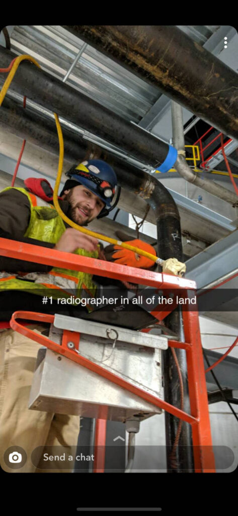
A mysterious (but very skilled) radiographer using a gamma isotope & film to radiograph pipe welds in the field
Automation & AI
With Film Radiography every piece of film is single use. Once the silver halide crystals are exposed they cannot be reverted back to their original state. The film must either be developed or discarded. This make Film Radiography inherently impractical for automating inspections.
Some time can be saved by using custom built fixtures or an automatic processor for the development process, but in general the image acquisition is a very manual and time consuming process.
Also, because Film Radiography is an analog process with a physical media for storing data; analysis of data cannot be aided with today’s AI computer vision models.
Film Exposure Example - Film, Part, IQIs, ID Tags must be placed for each exposure
In contrast with Digital Radiography, a DDA is reusable and can be integrated with PLCs to develop image acquisition programs which are fully automated and repeatable. This greatly saves time and cost of consumable materials when compared to Film Radiography.
These images can also be sent directly to computer vision models for analysis with AI. This is a capability that some NDT manufacturers are investing heavily into at the moment.
One of Industrial Inspection's Automated DR/CT Systems
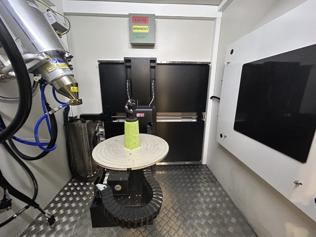
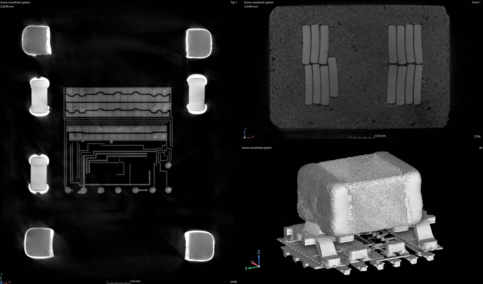
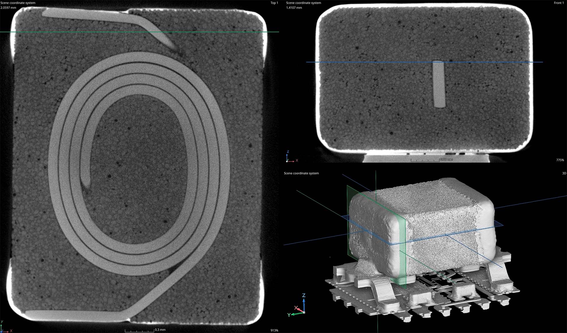
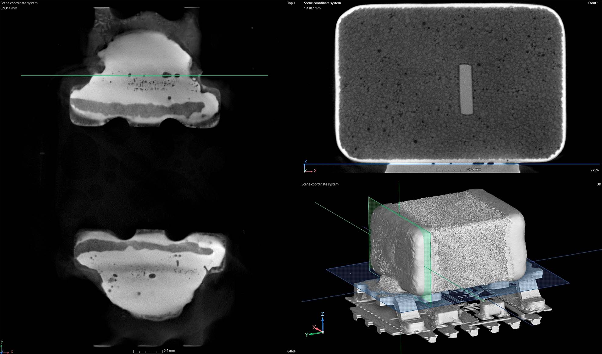
Micro-CT (micro-computed tomography) scanning has become an essential tool for inspecting microchips and PCBs (Printed Circuit Boards) in the electronics industry. The technology allows for non-destructive, high-resolution internal imaging, which is crucial for ensuring the quality and performance of microchips and PCBs.
Below are some CT scan images of a microchip and some beneficial reasons for CT scanning these critical components.
Preservation of Samples: Micro-CT scanning allows for the inspection of microchips and PCBs without physically damaging them. This is especially critical for high-value components or prototypes where any damage could lead to costly delays or failures.
Internal Inspection: Unlike traditional techniques, such as X-ray inspection, micro-CT allows for the detailed visualization of the internal structures of microchips, such as the bonding wires, die, and underfill, without disassembling the components.
Inspection of Assembly Integrity: In addition to inspecting individual microchips, micro-CT scanning is highly effective in checking the quality of the entire PCB assembly, including:
Placement accuracy of components (such as resistors, capacitors, and chips)
Via integrity (e.g., detecting voids or solder bridges in vias)
Trace continuity and checking for potential issues in signal paths or power distribution
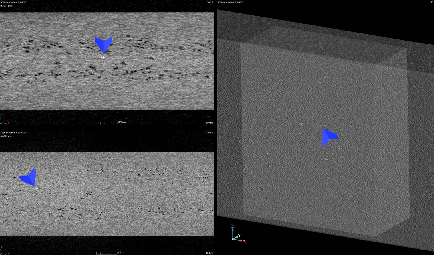
Micro-Solder Joint Inspection: Micro-CT is particularly valuable for examining solder joints, which are often located in hard-to-reach areas. It can check for the presence of solder voids, underfill problems, or even assess the amount of flux residue left over.
Failure Analysis: Micro-CT scanning can identify faults within microchips and PCBs that are invisible to the naked eye or traditional inspection methods, such as:
Solder joint failures (e.g., cracks, cold solder joints, or voids)
Delamination in multi-layer PCBs
Corrosion or oxidation within microchips
Process Optimization:
Feedback for Manufacturing Process: Data obtained from micro-CT scans can be used to fine-tune manufacturing processes. For example, if a high defect rate is found in a specific area of the PCB, the manufacturing process can be adjusted to address that issue and improve yield.
Supply Chain and Component Analysis: Micro-CT scanning can also be used to inspect incoming components from suppliers, verifying that they meet the required specifications and quality standards before they are incorporated into the final product.
In 2005, Hasbro launched a Star Wars collectible action figure game called Attacktix, which became a childhood obsession of mine. The game featured hundreds of characters to collect, each sold in mystery boxes containing three figures. Part of the excitement came from not knowing who you’d get until you opened the box at home, always hoping for a rare figure like Boba Fett.
Nowadays, there are all kinds of different mystery box toys on the market. I purchased 5 unique brands to see if we could use the power of attenuating radiation to see what is inside without opening them.
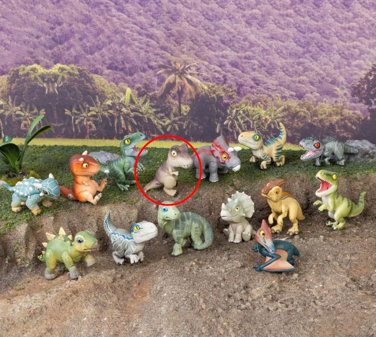
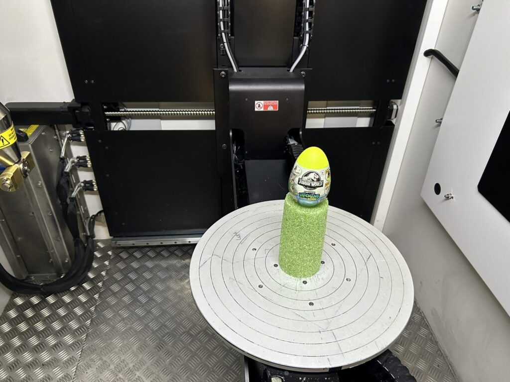
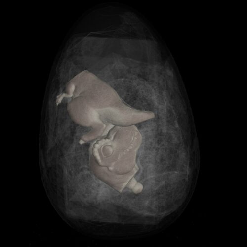
Starting off is Jurrasic World Captivz Hatchling Dinos.
CT scanning showed some paper, sand, & a plastic figurine. After isolating the figurine, and matching the features of the jaw & the tail it became clear that it was the brown/tan baby t-rex.
Dinosaur Egg in the CT Scanner!
Isolated 3D CT Model of Baby T-Rex
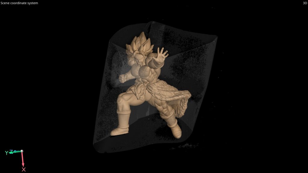
Next up is the Dragon Battle Figure Series. This one has 5 different possible figures. Using CT scanning we isolated the figure inside the pouch. Based on his pose it is clear that this one is the legendary Super Saiyan himself, Broly!
Isolated 3D CT Model of Broly
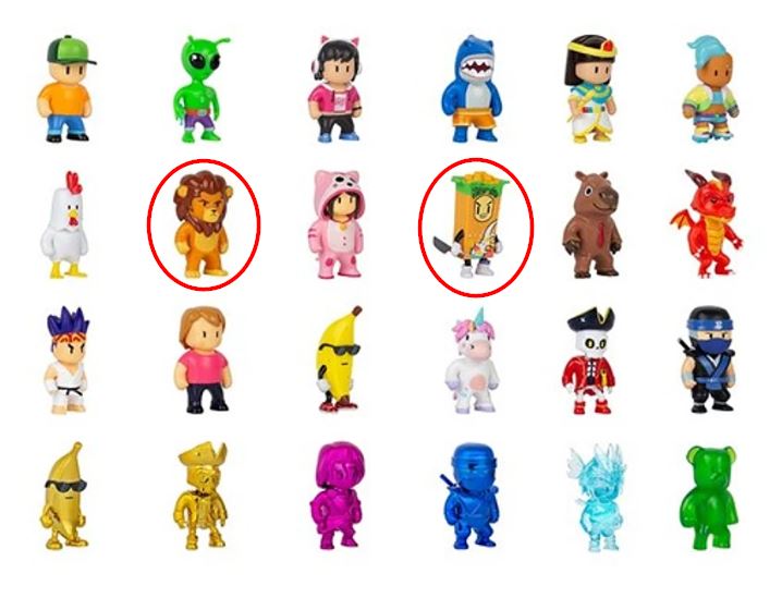
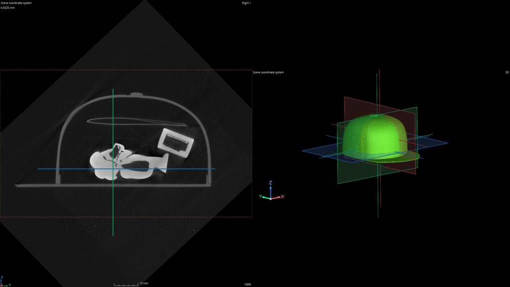
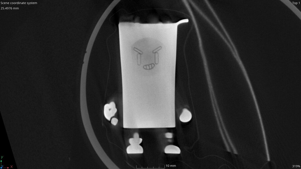
Now on to the Stumble Guys. This cool green hat packaging comes with 2 unique figurines inside. Rather than isolating the 3D models, I relied on the 2D views for this one. I was able to find a figure that looked like a lion and one that looked like a box of cereal. This can only be ‘Leonidas’ & ‘Killer Size’.
Cross Section of Leonidas & 3D Model of the Hat
Front Section of Killer Size - Check out the face details!
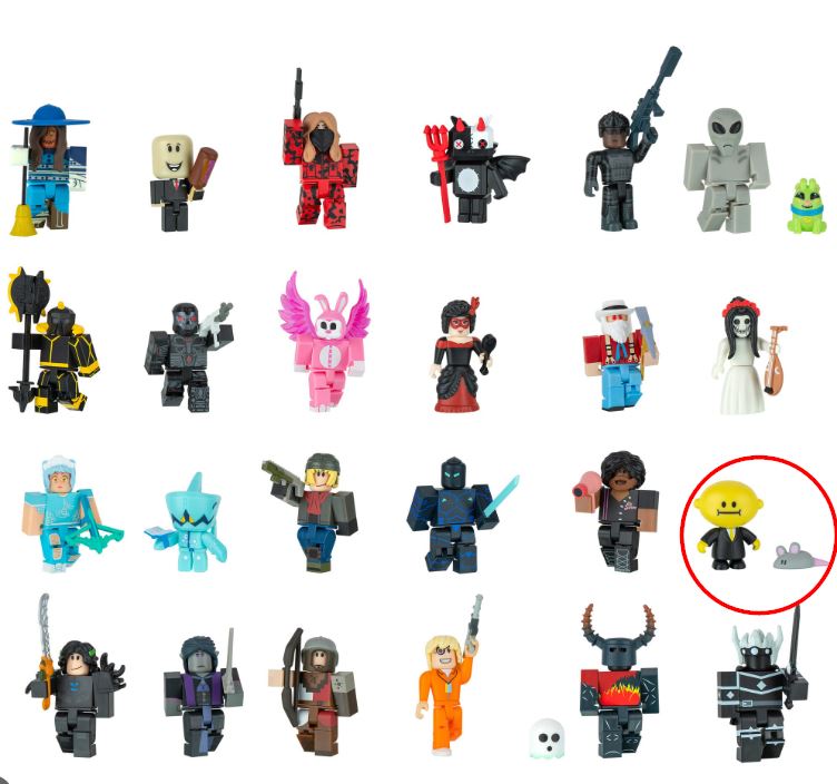
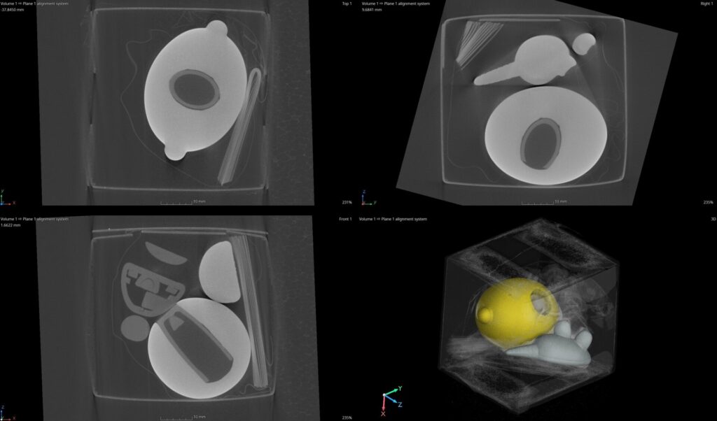
Onto Roblox. Here we CT scanned a mystery figure from Series 12. I was confused when I first opened up the file. I just saw a big oval, after doing a little digging it was clear it could only be ‘Lemon Head’. He got that skibidi toilet rizz.
2D Slice Planes & 3D Model of Mr. Lemon Head & His Mouse
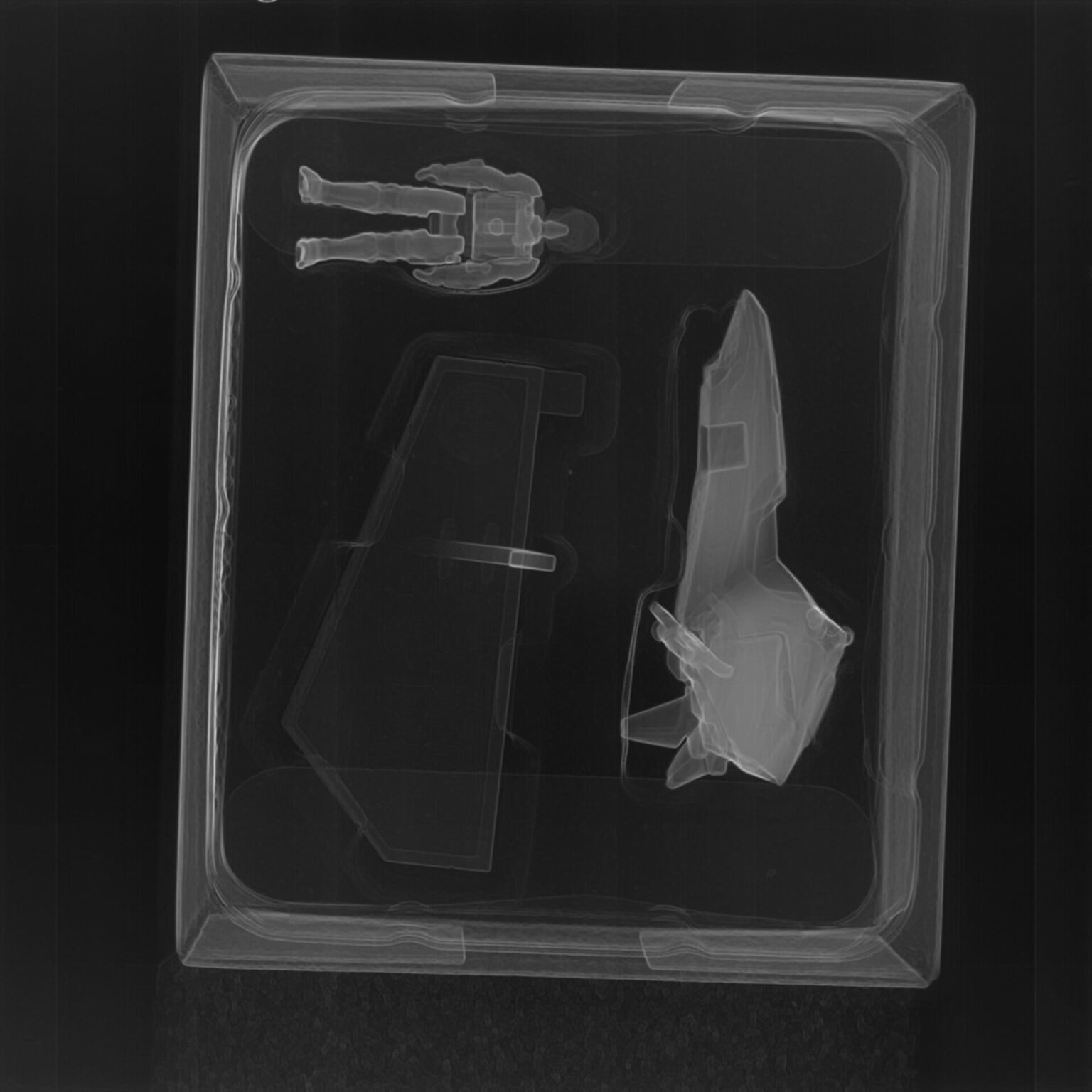
Lastly is a Series 5 set from Star Wars Micro Galaxy Squadron. At this point I decided to challenge myself and see if I could detect what was inside with just a single, quick 10 second x-ray image. I had a hard time telling by the figurine alone, but the features of the speeder made it obvious that this is the blue mandalorian.
2D X-ray of Box Showing Figurine, Speeder, & Base Inside
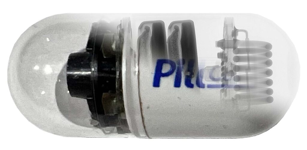
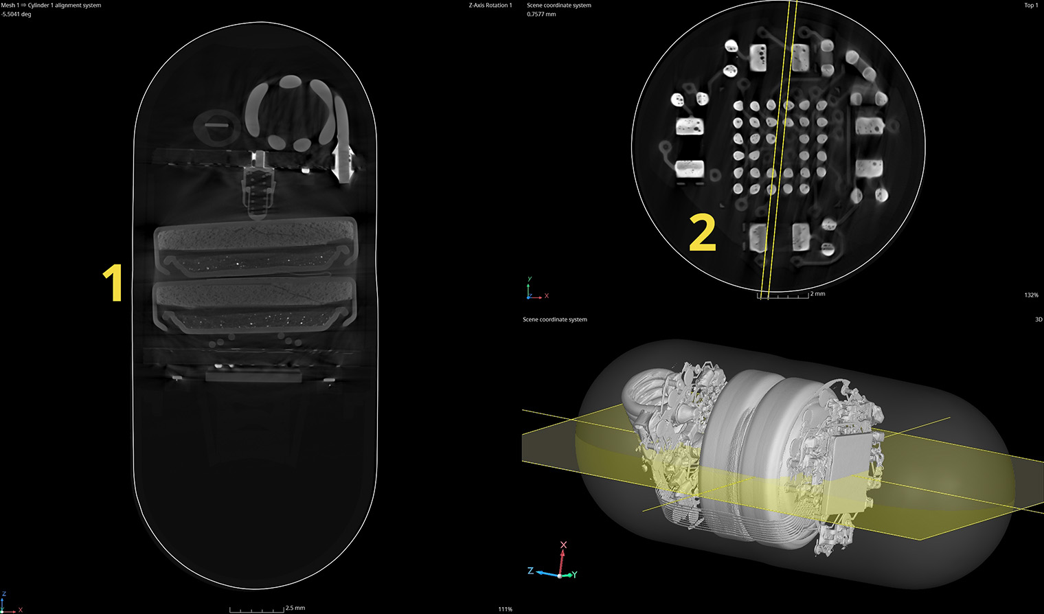
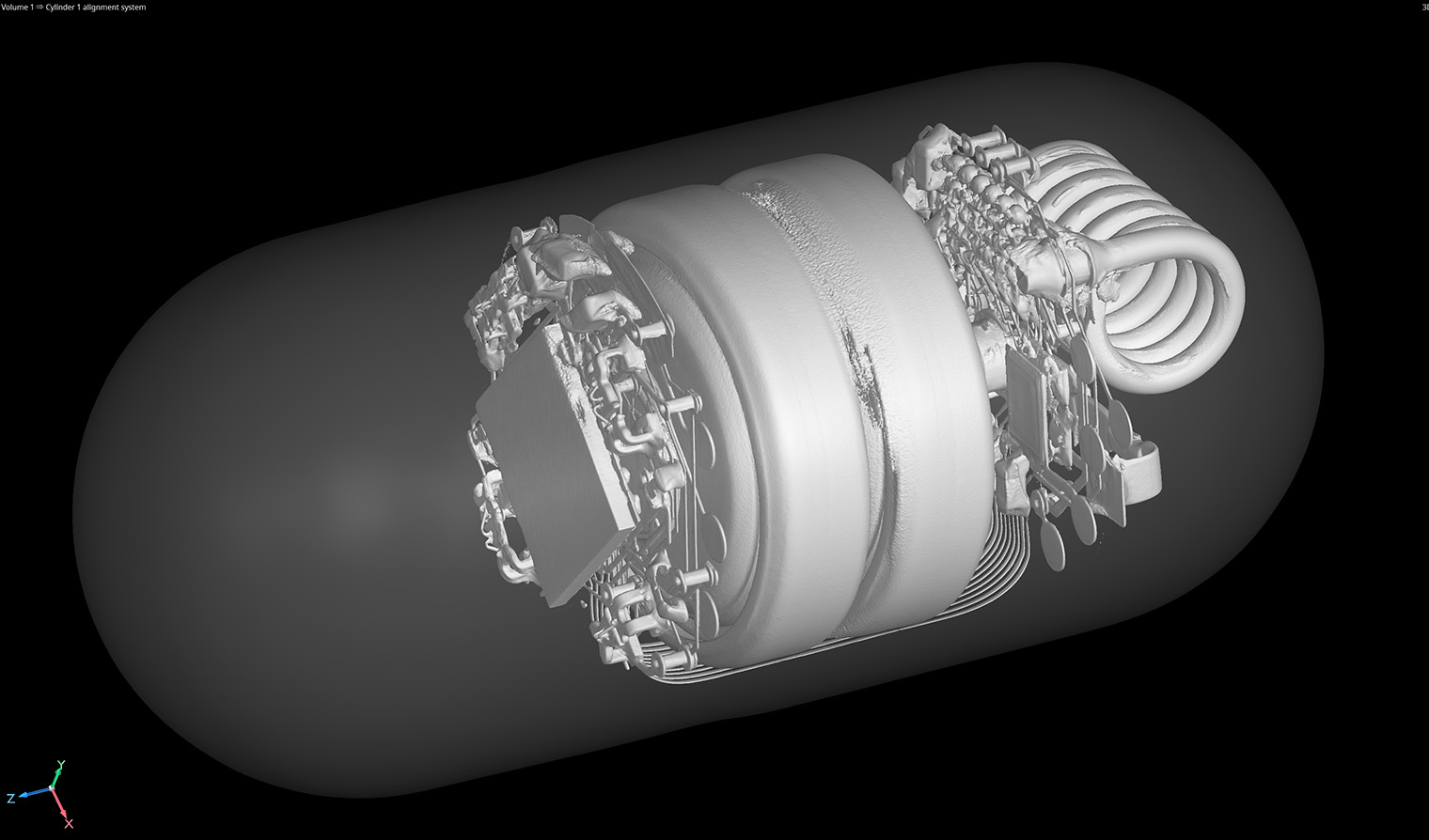
Pill cameras, or “pillcams,” are small, ingestible devices used to capture images of the inside of the gastrointestinal tract. They are particularly useful for diagnosing conditions like Crohn’s disease, ulcers, and cancers in areas that are hard to reach with traditional endoscopy, such as the small intestine. The main benefit of pillcams is that they offer a minimally invasive, comfortable alternative to more traditional procedures, allowing doctors to observe the GI tract in real time as the pill moves through the system.
Industrial CT scans can assess the alignment and assembly of small, complex parts inside medical devices like pillcams, ensuring that all components are correctly positioned and functioning as intended. This technology offers high-resolution 3D imaging, allowing for precise analysis of intricate details that would be difficult to detect with traditional inspection methods like X-ray or visual inspection. Thus, CT scanning plays a critical role in ensuring that medical devices meet safety, performance, and quality standards before being released for use.
Battery evaluation for alignments, connections, and spring contact
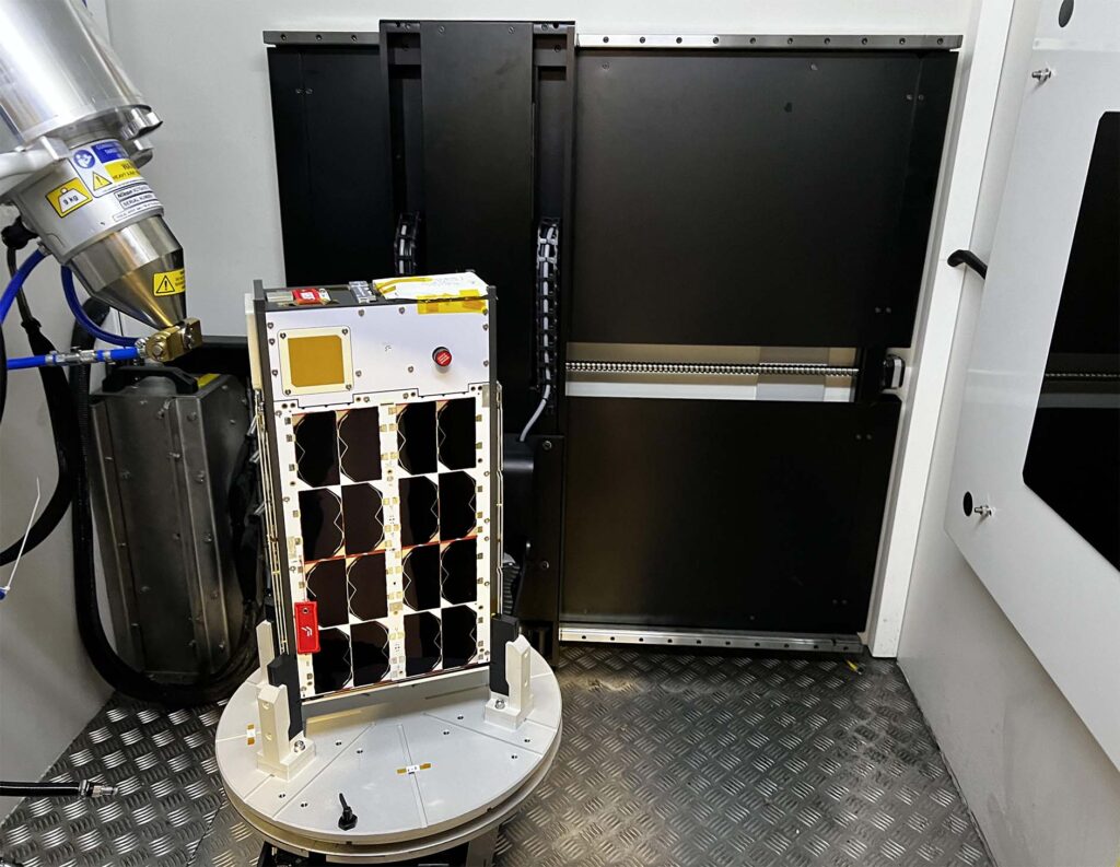
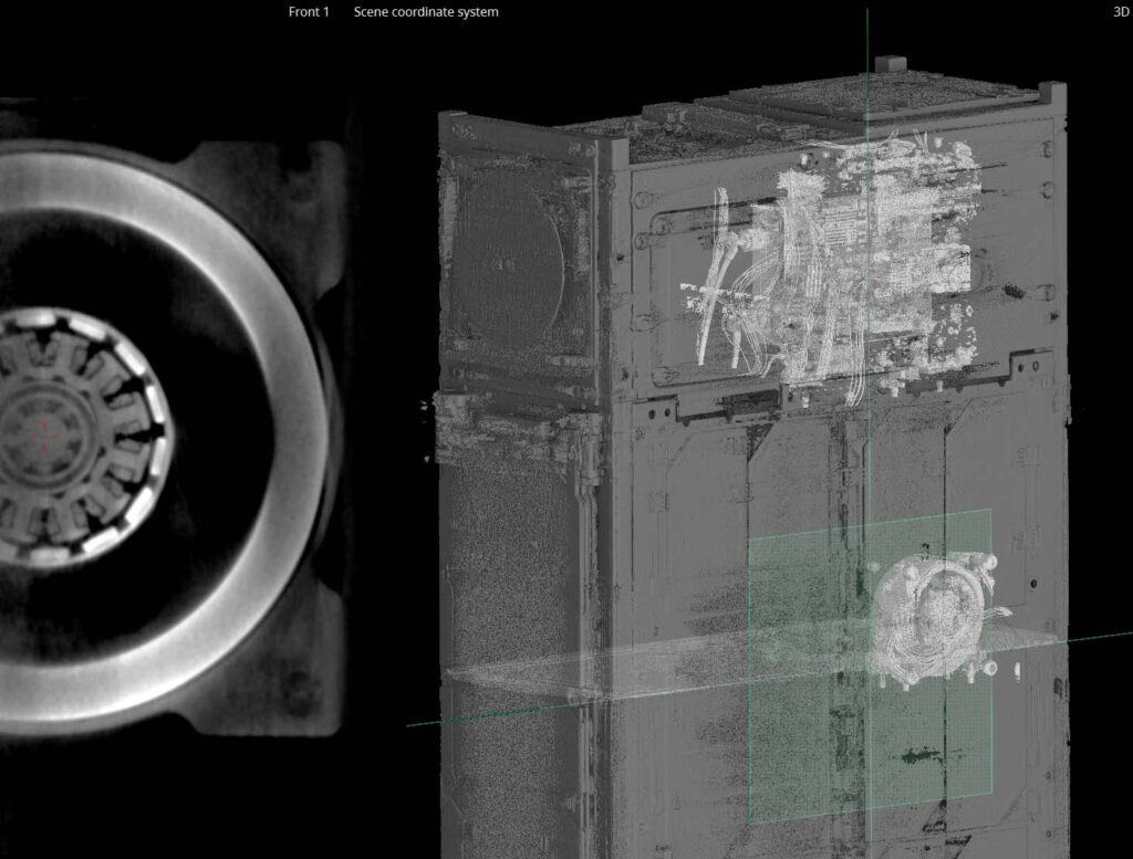
Industrial Inspection played a critical role in diagnosing a failure within this CubeSat. Set to launch on a SpaceX rideshare in November 2024, our client walked into our lab with a defective, seven-figure satellite and walked out with a plan for repair. We were challenged to determine the defect within one day so that build technicians would have enough time to tear down and repair or replace necessary components. Armed with only suggestions of possible zones for failure, our certified experts took on the challenge of finding this needle in a haystack.
“Our staff is comprised of world class inspection experts hailing from renowned inspection labs, space companies, and defense contractors. We thrive under pressure and perform at our best when failure is not an option,” said Keith Irwin, Managing Partner of Industrial Inspection.
THE CHALLENGE
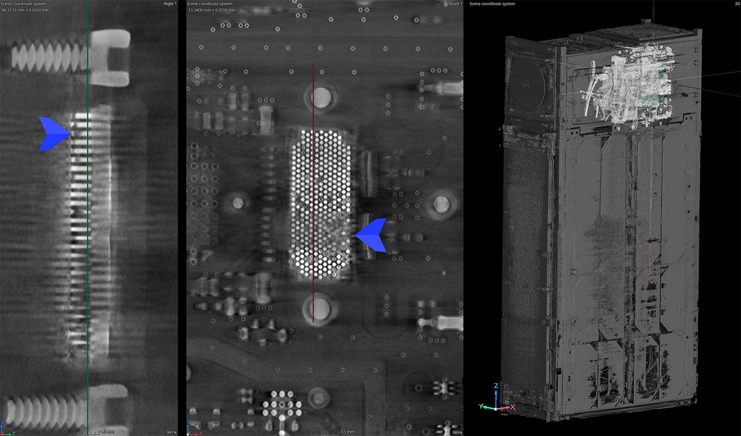
Large, complex systems like this CubeSat present a variety of challenges for Industrial X-Ray Imaging & CT Scanning. For example, opposing parameters like resolution versus energy must be weighed for their pros and cons. Without enough energy there would be a lack of penetration and increased x-ray artifacts. But, higher energy also introduces a larger x-ray spot-size and reduced resolution.
When imaging PCBs and searching for cracks or foreign object debris, resolution reigns supreme. Because of this, we swapped our 320kv mesofocus x-ray source (>30um resolution) out for our 225kv microfocus source (>3um resolution) in our large format x-ray cabinet. In order to locate any potential defects we must work through increased noise and artifacts to find miniscule defects.
Below is the point of failure – the signal amplifier likely overheated causing fracture. The left image shows a cross-sectional view through the side of the component, the middle view shows a top-down cross-section, and the right view shows the 3D render with the location of the component.
REACTION WHEEL IMAGING
Other areas of the satellite were also imaged for general information purpose like this reaction wheel and its copper windings.
Powered by batteries energized by small solar panels, reaction wheels are the preferred method for attitude control and stabilization. When a wheel spins, it creates angular momentum in one direction, causing the spacecraft to rotate in the opposite direction. By changing the speed of the wheels, the satellite can control its orientation in space without using propellant. This is particularly useful for precise pointing of instrumentation without the need for propellant.
All information has been shared with permission by our client.
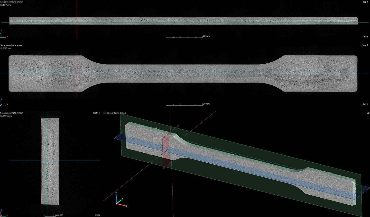
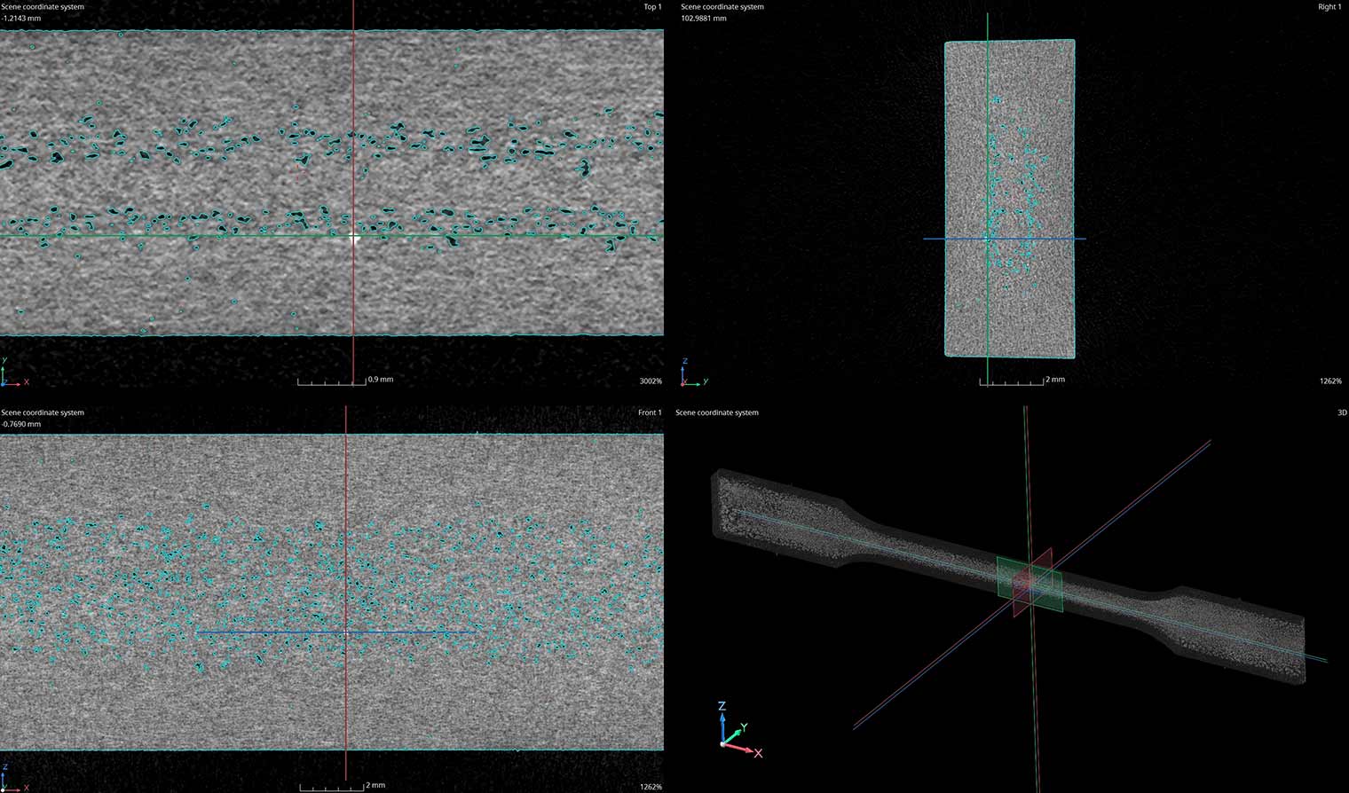
Tensile strips are manufactured materials used to measure or apply tensile stress in various applications. They are often used in structural engineering and material testing to evaluate the strength and elasticity of materials under tension. They come in a variety of shapes, sizes, and materials.
However, the sample in this case study is for a different purpose. While some manufacturers look to eliminate as much porosity as possible, others attempt to create a distribution of porosity for reasons like: flexibility, sound absorption, thermal insulation, and product lightening.
Industrial CT Scanning is used to characterize, quantify, and create 3D representations of these strips for failure analysis and FEA. Data can be exported into a variety of file formats.
100gb High Resolution Helical Scan of Tensile Strip
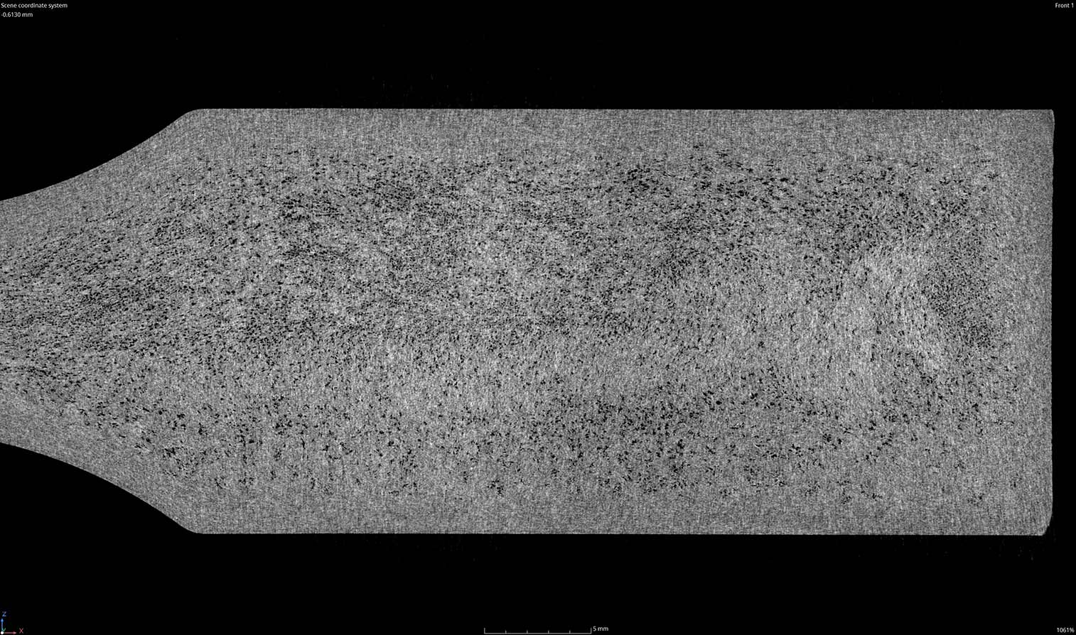
1000% ZOOM ON DATA - POROSITY & RESIN ORIENTATION WITNESSED
HIGH DENSITY INCLUSIONS EXTRACTED AND MAPPED
POROSITY CAN BE SEGMENTATED AND CALCULATED FOR TOTAL OR INDIVIDUAL PORE VOLUME
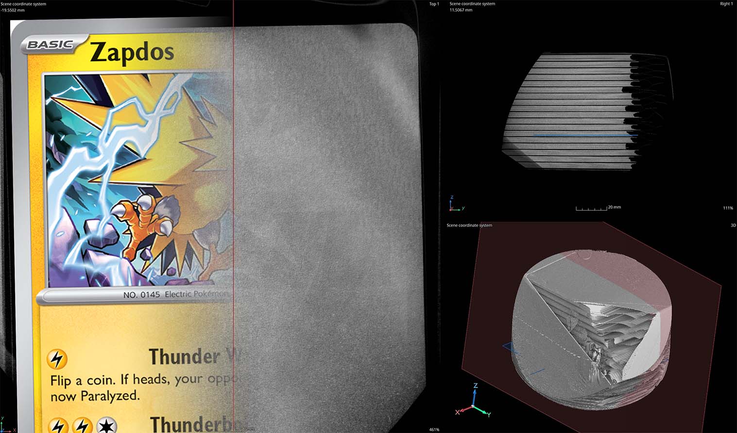
UPDATE 8/3/2024: We are aware of and working through the moral dilemma of CT scanning sealed collectibles. Our objective position is one of scientific ability and data-driven results. It is not our responsibility to determine the ethical positions and choices of others and we do not accept responsibility for their actions. 1. We have brought awareness to the entire industry of the existence and capabilities of this technology; it is up to individuals to make informed decisions moving forward. 2. In light of information we have received from industry insiders, we believe companies are using this technology in secret to take advantage of the collectibles market. 3. We are making this technology accessible to everyone rather than to just a minority. 4. We are working on policies to combat deceptive practices. 5. We are working on partnering with manufacturers to develop packaging security solutions. 6. We will continue to consider every request we receive. 7. This technology is here to stay and there will probably be additional companies offering it as a service at some time in the future. 8. The majority of requests we have received have been from people curious about the value of their “30 year old collectible” and if this is their opportunity for a life changing moment.
INDUSTRIAL INSPECTION BECOMES THE WORLD'S FIRST COLLECTOR CARD CT SCANNING SERVICE
First, we made public what’s been happening in secret. Now, we are bringing x-ray vision to the masses – quickly, affordably, and reliably. Preserve your investments, maintain your edge against wealthy investors and bad actors, and understand the value of what you own. We can image everything from packs to booster boxes for sports and card games.
To learn more check out our Collector Card CT Scanning Page here:
Inspecting Additively Manufactured Components using Industrial CT Scanning
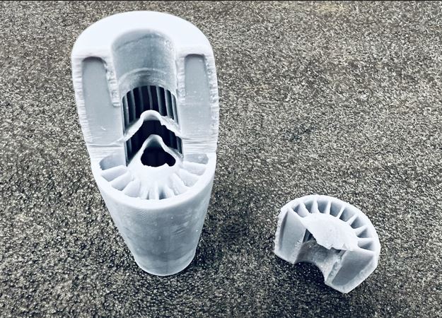
Additive manufacturing (3D printing) allows for the creation of highly complex and intricate designs that would be difficult or impossible to achieve with traditional manufacturing methods. This includes features like internal channels, lattice structures, and custom geometries. Because these complex designs are typically internal, their inspection is also extremely difficult or impossible. One option is to physically cut the part, but this introduces a variety of consequences. Another option, and the purpose of this case study, is to digitally cut through the sample using Industrial CT Scanning technology. CT Scanning allows us to capture highly accurate data for the inspection of internal and external geometry of a variety of components.
Part sectioned to photograph internal profiles
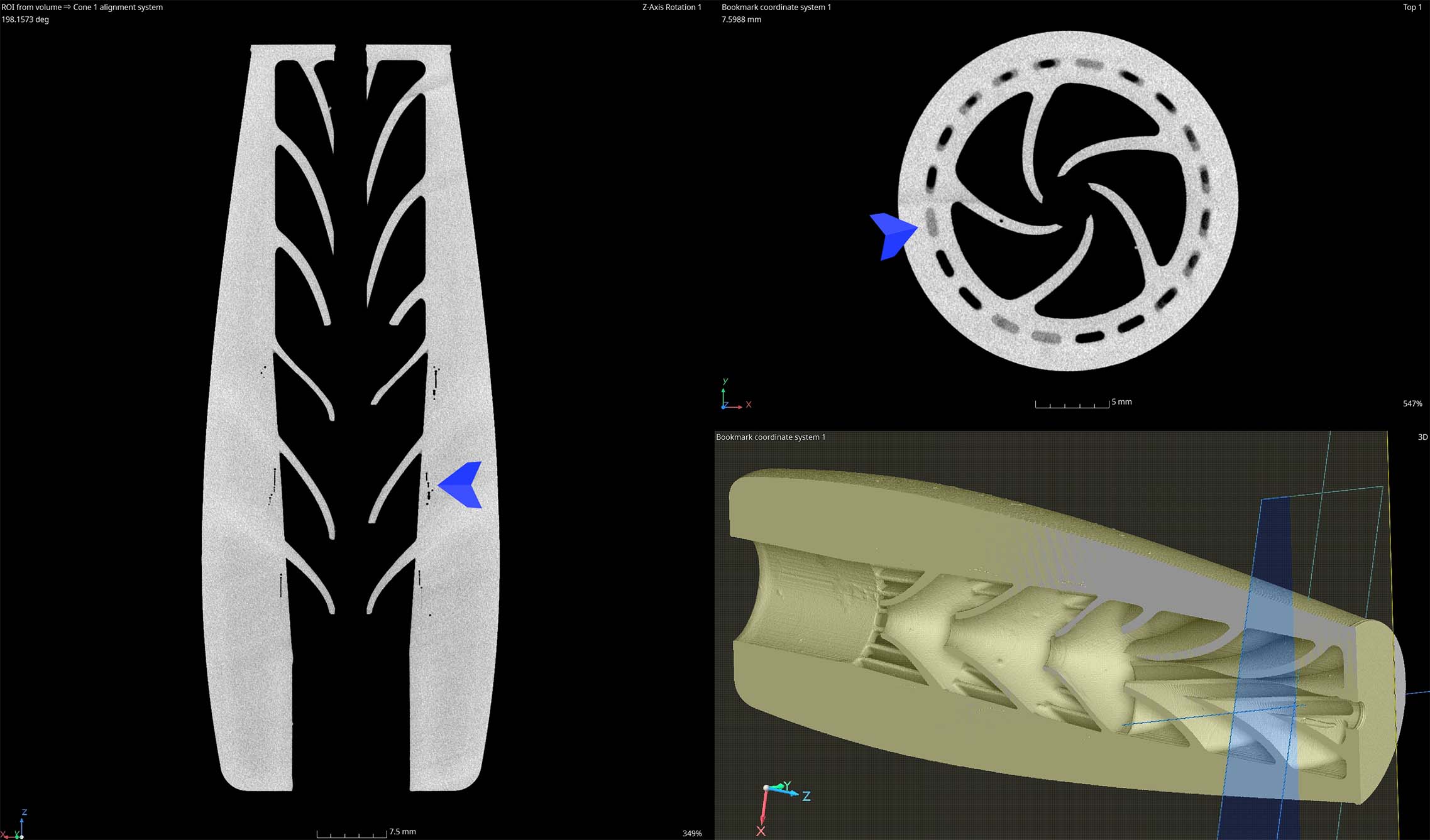
ROTATIONAL VIEWING METHOD
Cylindrical parts like this can be viewed about an axis. A cylinder is defined and then the viewing pane rotates about that axis to show inconsistencies and indications. The left arrow shows vertical build failures. The right arrow shows trapped build material.
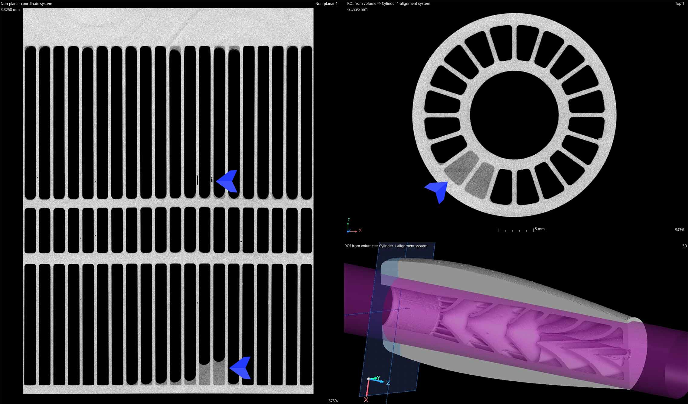
UNROLL VIEWING METHOD
For an alternative look at internal geometries, a cylindrical feature can be “unrolled” into a planar view. Image a toilet paper roll cut down one side and laid flat on a table. This offers the viewer the opportunity to simultaneously view a given offset from an axis.
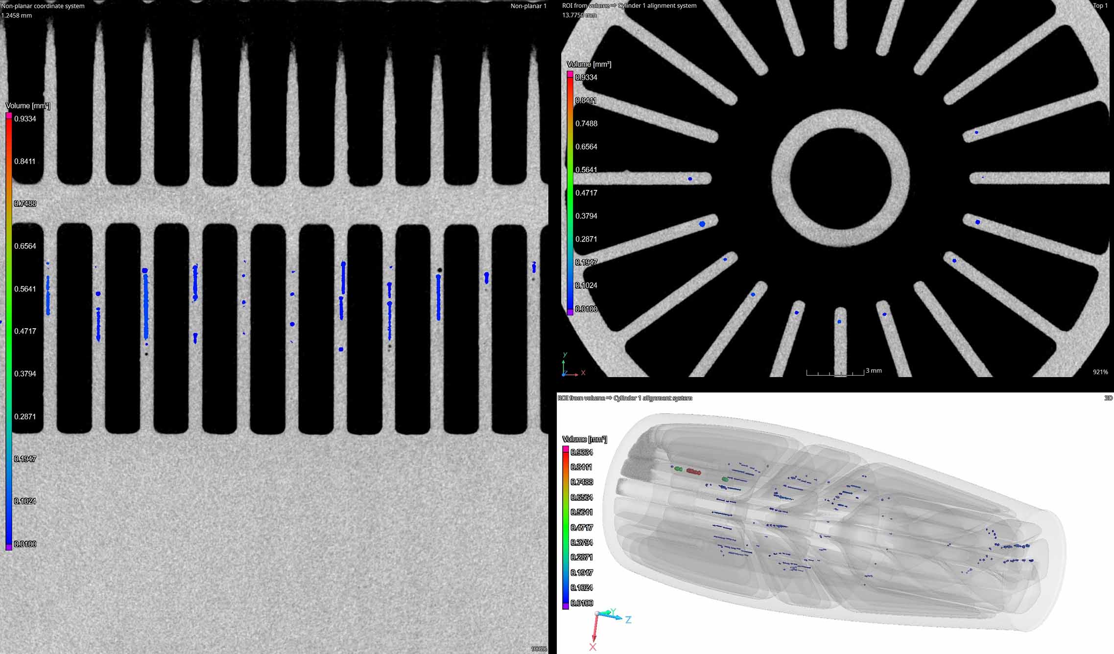
VOLUMETRIC POROSITY CALCULATIONS
Porosity and inclusions can be extracted and calculated for volume, spherical diameter, and other characteristics. This information can be used to qualify parts or amend manufacturing parameters for better parts.
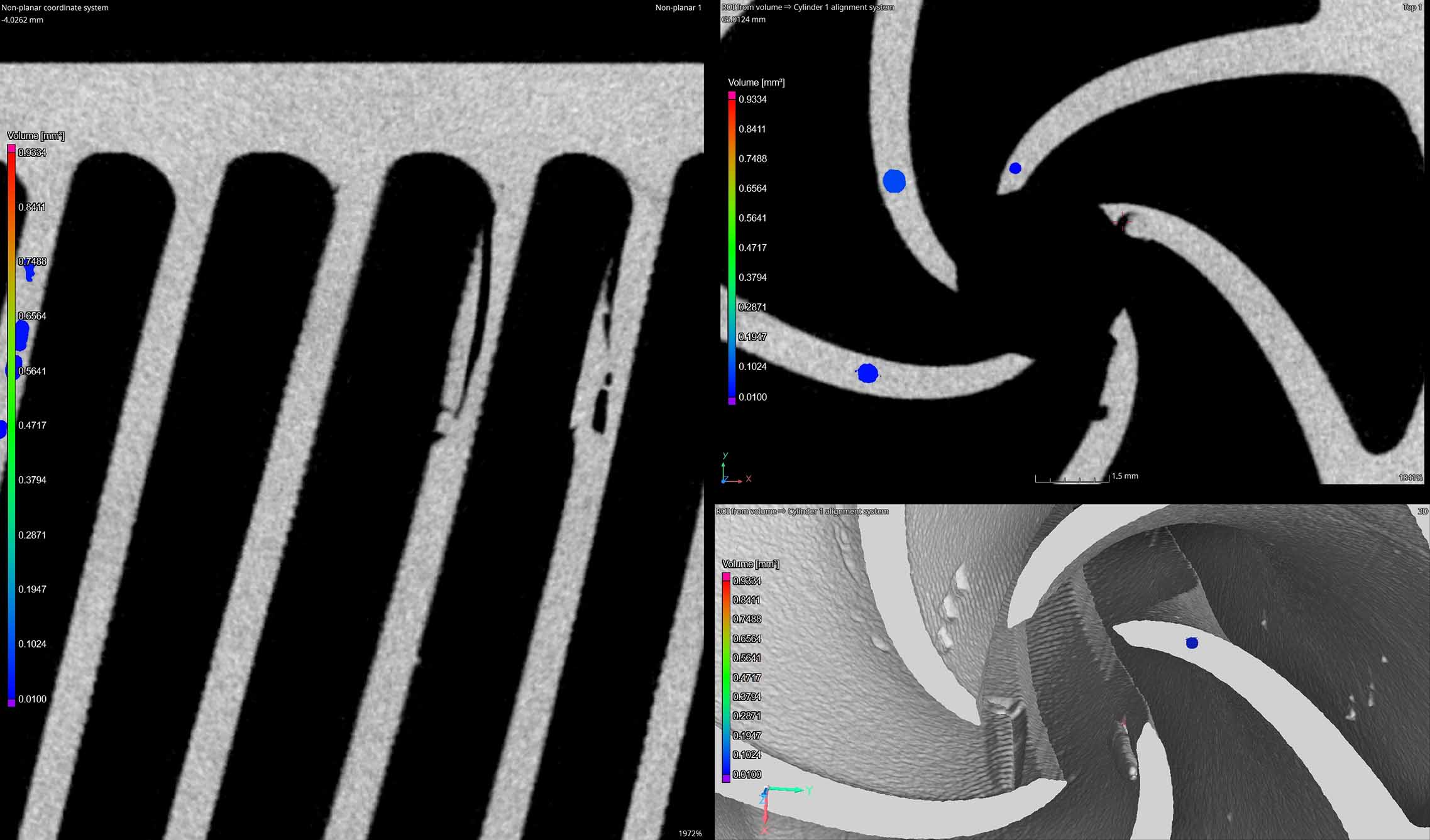
BUILD DEFECT LOCATING AND IMAGING
Internal build failures can be located and evaluated before the component makes it into the field.