Skip to content
Home
About
Services
Industrial CT Scanning Services
Collectibles CT Scanning Service
Digital X-Ray Services (DR)
3D Scanning & Metrology
CMM Services
2D & 3D Vision & Optical Profilometer Services
Reverse Engineering Services
3D Printing & Fixturing
Dye Penetrant Testing Services (PT)
Ultrasonic Testing (UT)
Eddy Current Testing Services
Visual Testing Services (VT)
Magnetic Particle Testing Services (MT)
NDT Consulting & Oversight
Training & Certifications Services >
Training Course List
X-Ray Film & Image Review Services
Resources
Case Studies
Industrial CT Scanning Case Studies
Industrial X-Ray Case Studies
3D Scanning & Reverse Engineering Case Studies
Guides
X-Ray Safari
Contact
sales@industrialinspection.com
(231)246-8473
Month: March 2024
FOD & Potting Failure in Probe
March 10, 2024
/
X-Ray & CT Scanning
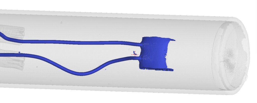
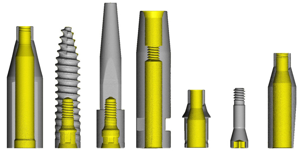
Inspecting Surgical Screws using Industrial CT Scanning
March 9, 2024
/
Reverse Engineering
,
X-Ray & CT Scanning
Industrial Inspection is ITAR Registered
March 2, 2024
/
News