CT Scanning PCB Microchips
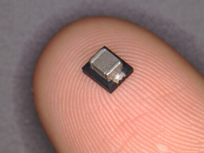
Micro-CT (micro-computed tomography) scanning has become an essential tool for inspecting microchips and PCBs (Printed Circuit Boards) in the electronics industry. The technology allows for non-destructive, high-resolution internal imaging, which is crucial for ensuring the quality and performance of microchips and PCBs.
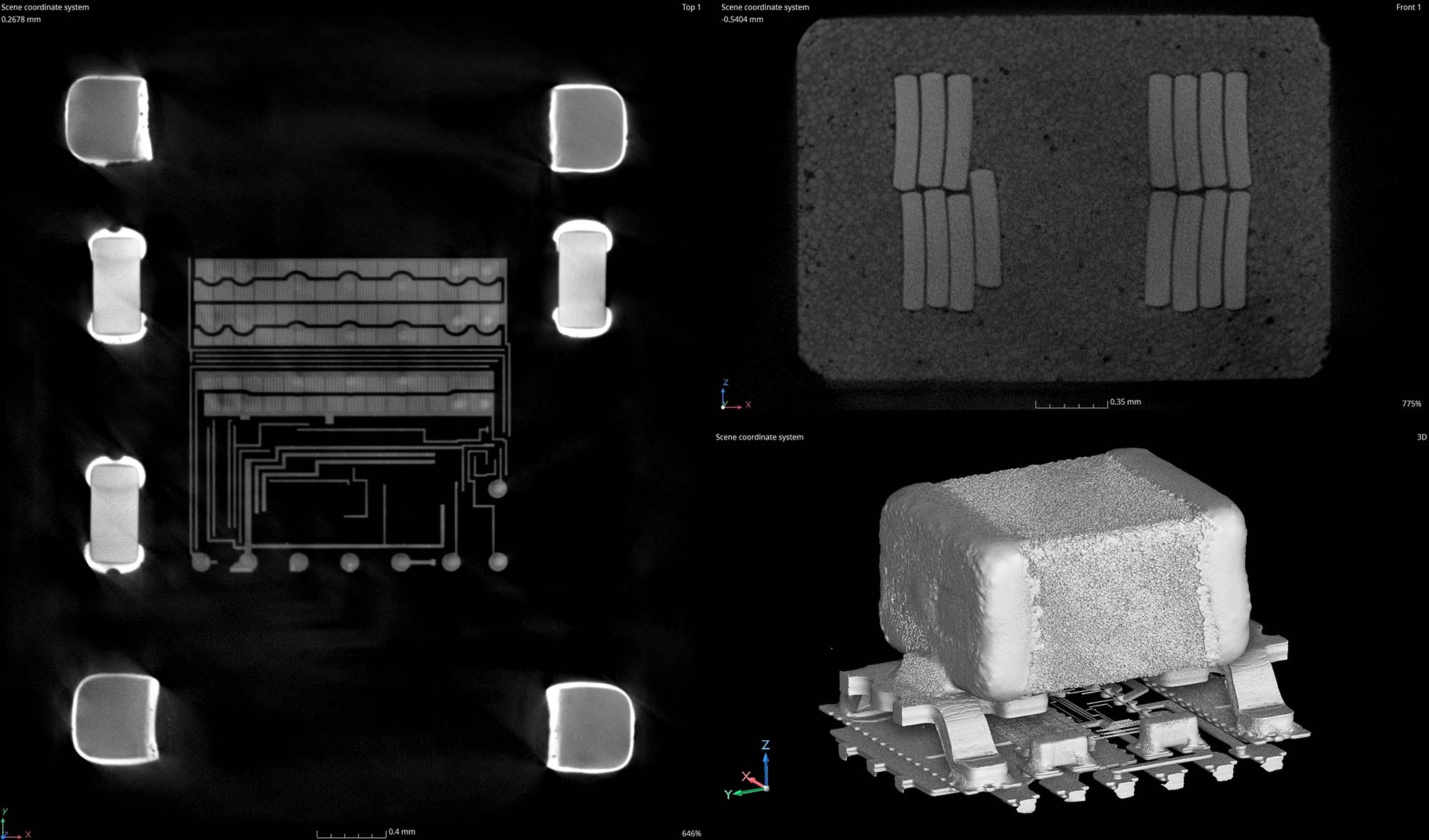
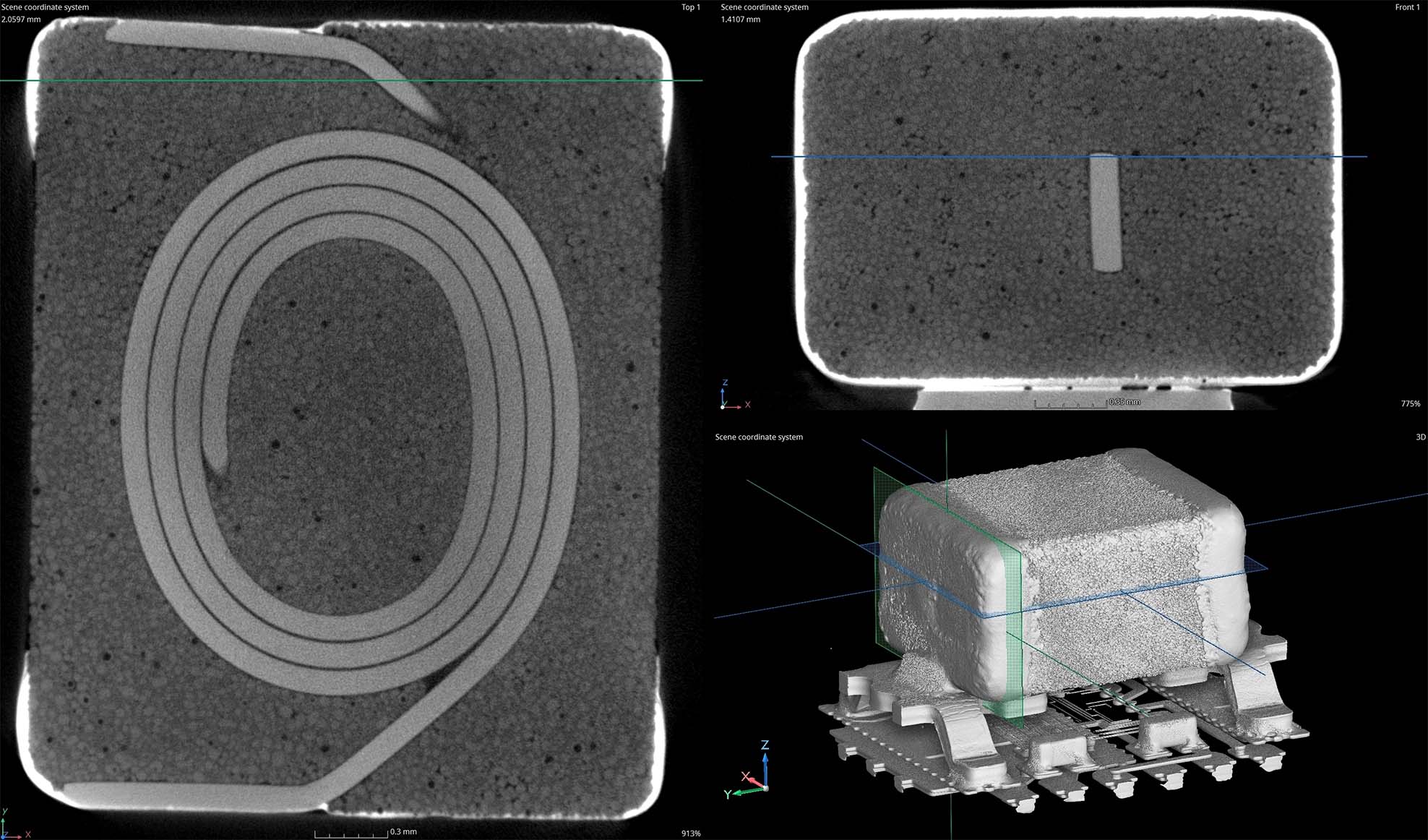
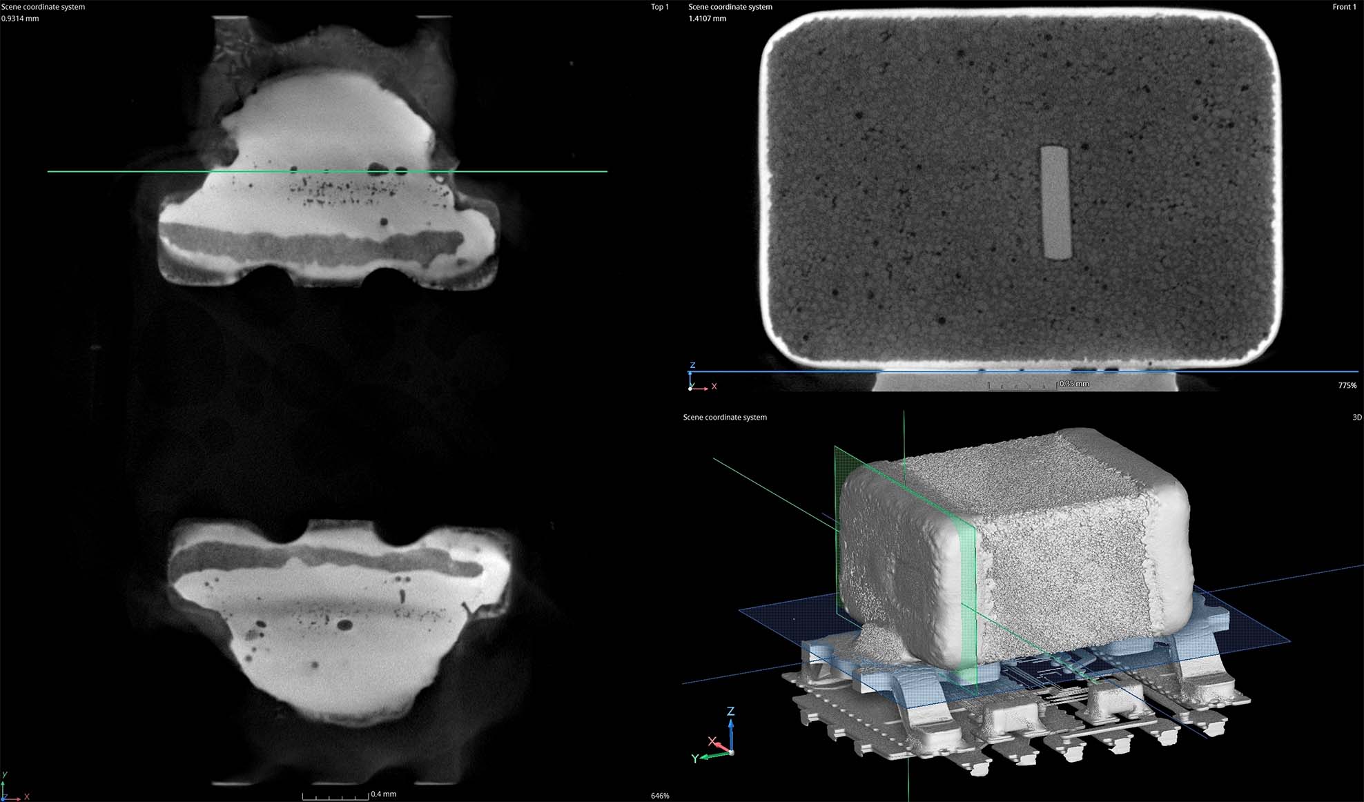
Below are some CT scan images of a microchip and some beneficial reasons for CT scanning these critical components.


- Preservation of Samples: Micro-CT scanning allows for the inspection of microchips and PCBs without physically damaging them. This is especially critical for high-value components or prototypes where any damage could lead to costly delays or failures.
- Internal Inspection: Unlike traditional techniques, such as X-ray inspection, micro-CT allows for the detailed visualization of the internal structures of microchips, such as the bonding wires, die, and underfill, without disassembling the components.
- Inspection of Assembly Integrity: In addition to inspecting individual microchips, micro-CT scanning is highly effective in checking the quality of the entire PCB assembly, including:
- Placement accuracy of components (such as resistors, capacitors, and chips)
- Via integrity (e.g., detecting voids or solder bridges in vias)
- Trace continuity and checking for potential issues in signal paths or power distribution
- Micro-Solder Joint Inspection: Micro-CT is particularly valuable for examining solder joints, which are often located in hard-to-reach areas. It can check for the presence of solder voids, underfill problems, or even assess the amount of flux residue left over.
- Failure Analysis: Micro-CT scanning can identify faults within microchips and PCBs that are invisible to the naked eye or traditional inspection methods, such as:
- Solder joint failures (e.g., cracks, cold solder joints, or voids)
- Delamination in multi-layer PCBs
- Corrosion or oxidation within microchips
- Process Optimization:
- Feedback for Manufacturing Process: Data obtained from micro-CT scans can be used to fine-tune manufacturing processes. For example, if a high defect rate is found in a specific area of the PCB, the manufacturing process can be adjusted to address that issue and improve yield.
- Supply Chain and Component Analysis: Micro-CT scanning can also be used to inspect incoming components from suppliers, verifying that they meet the required specifications and quality standards before they are incorporated into the final product.
