Industrial X-Ray & CT scanning is used to non-destructively evaluate printed circuit boards.
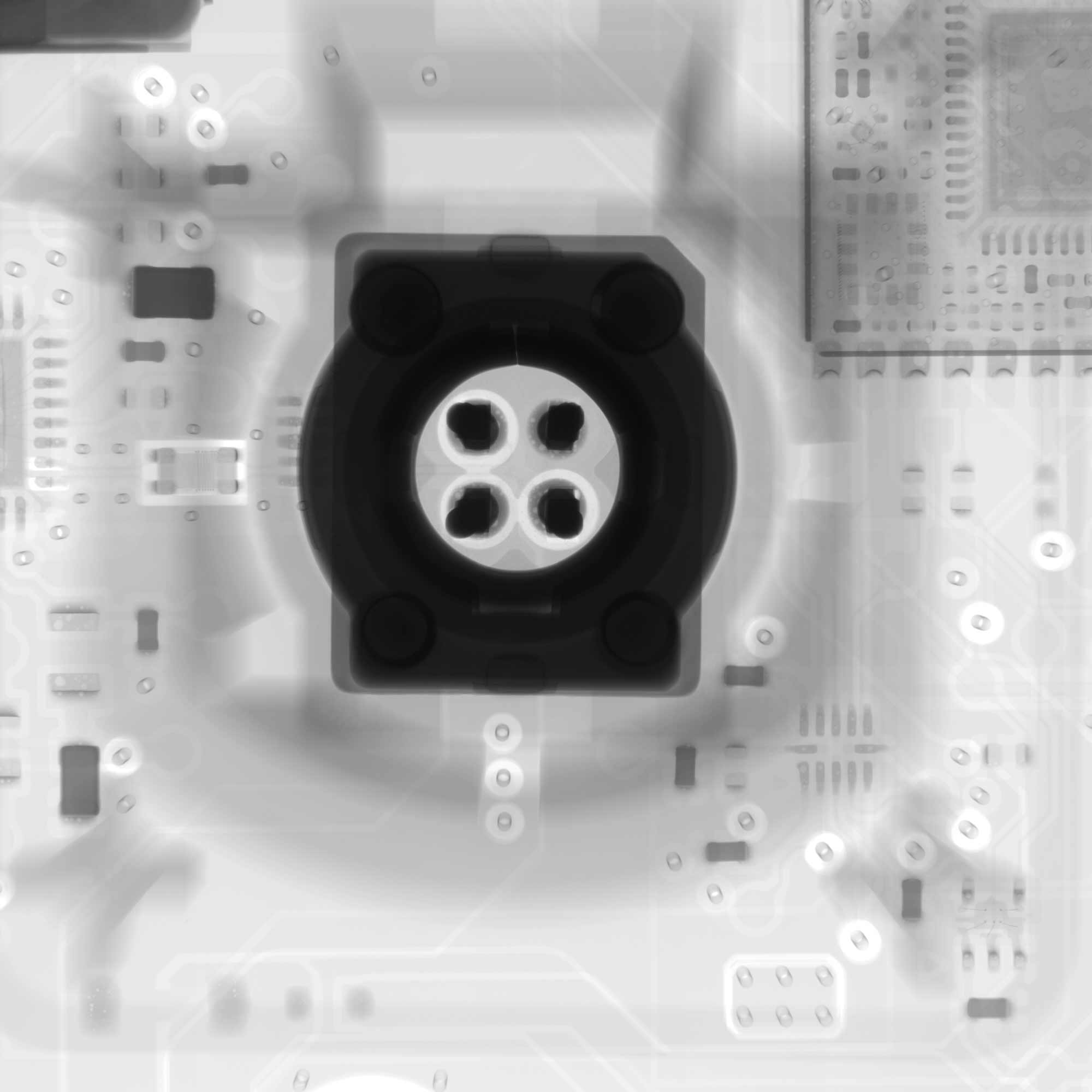
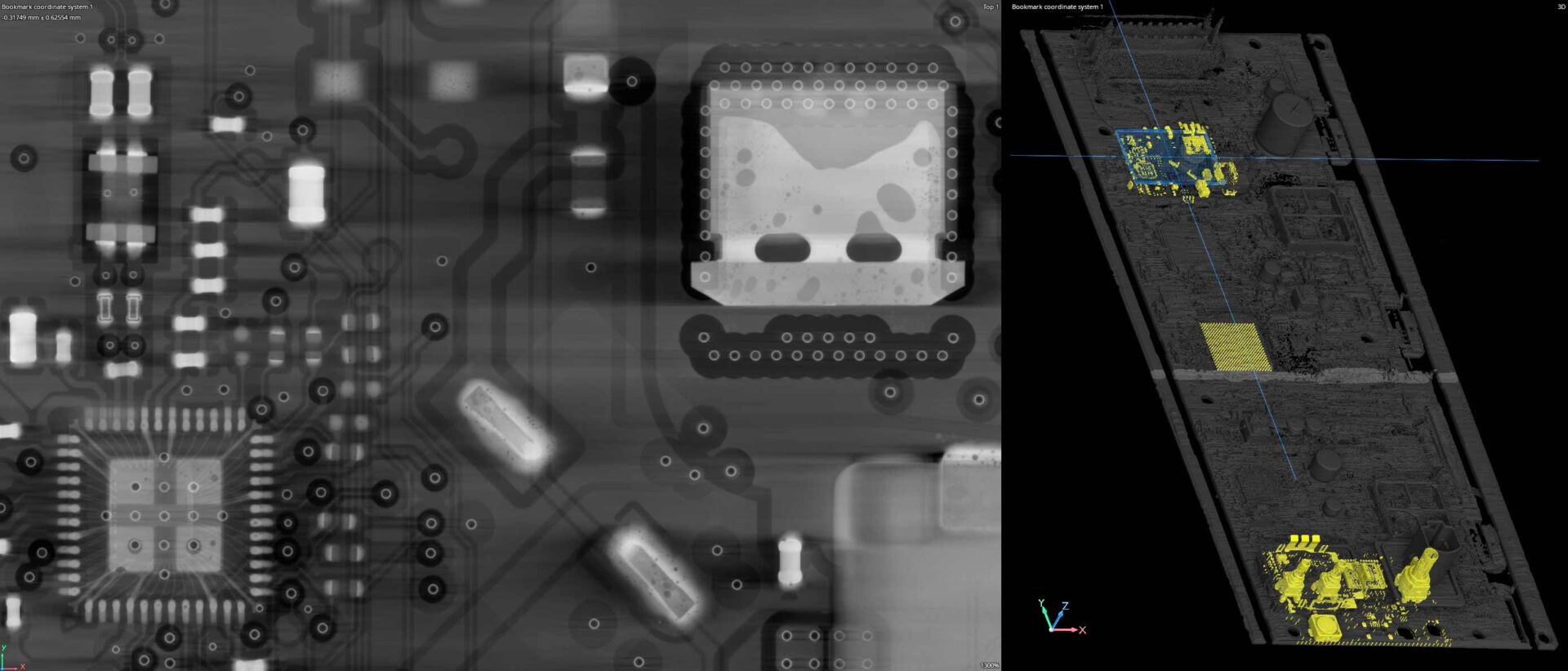
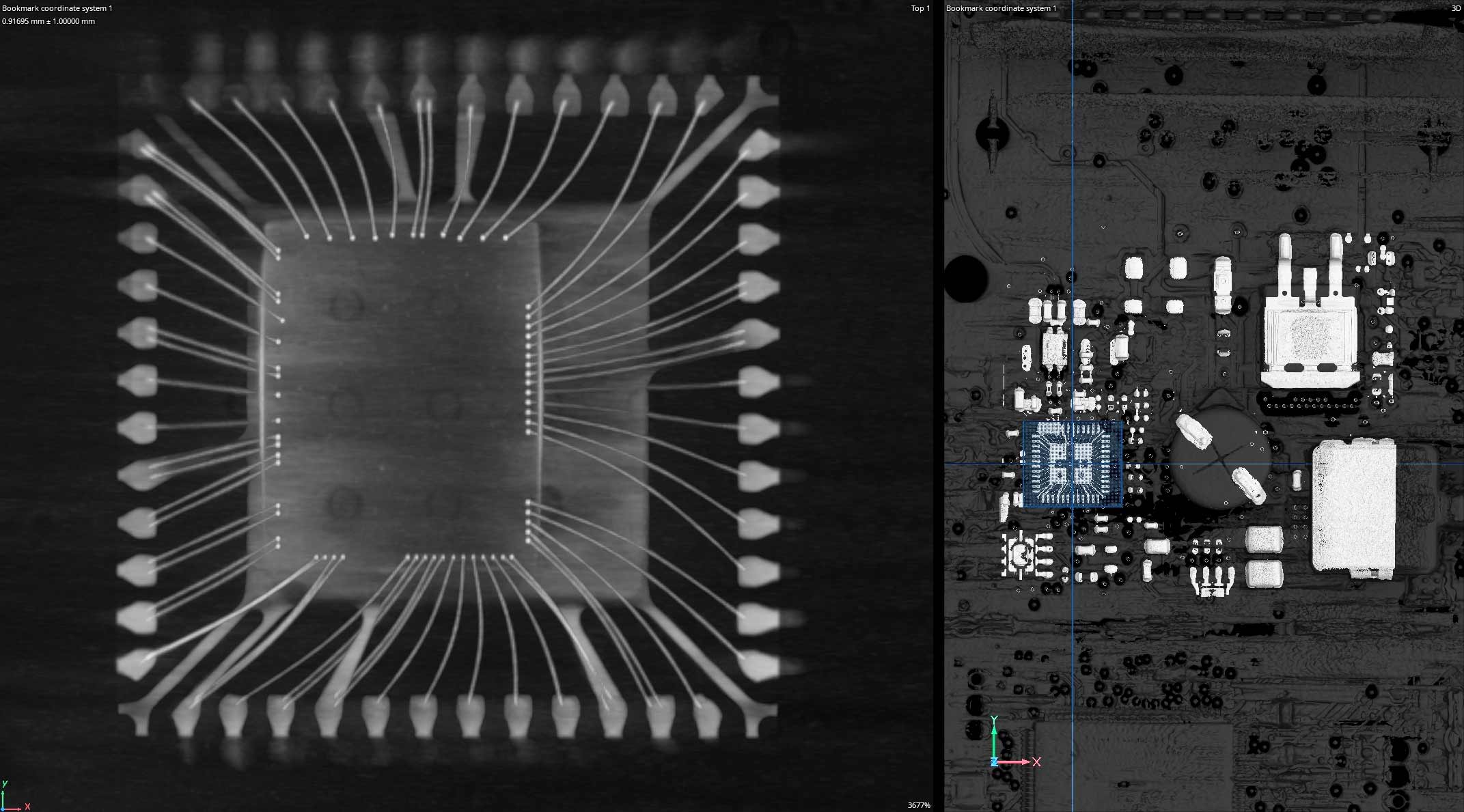
2D X-RAY
2D x-ray allows our certified technicians to quickly inspect features like bond wire straightness, pin perpendiculariy, BGA porosity, trace defects, and capacitor cracks. Our high resolution systems are fully programmable allowing automated image acquisition including translations, rotations, and magnification changes.
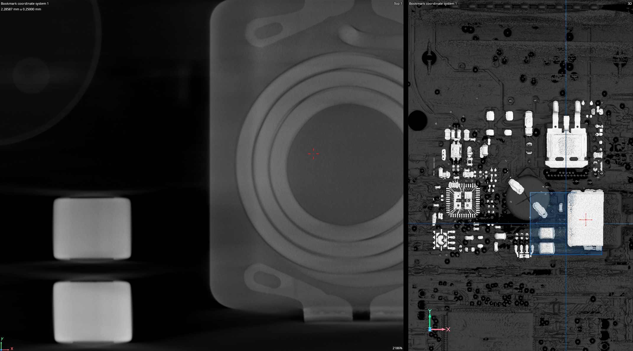
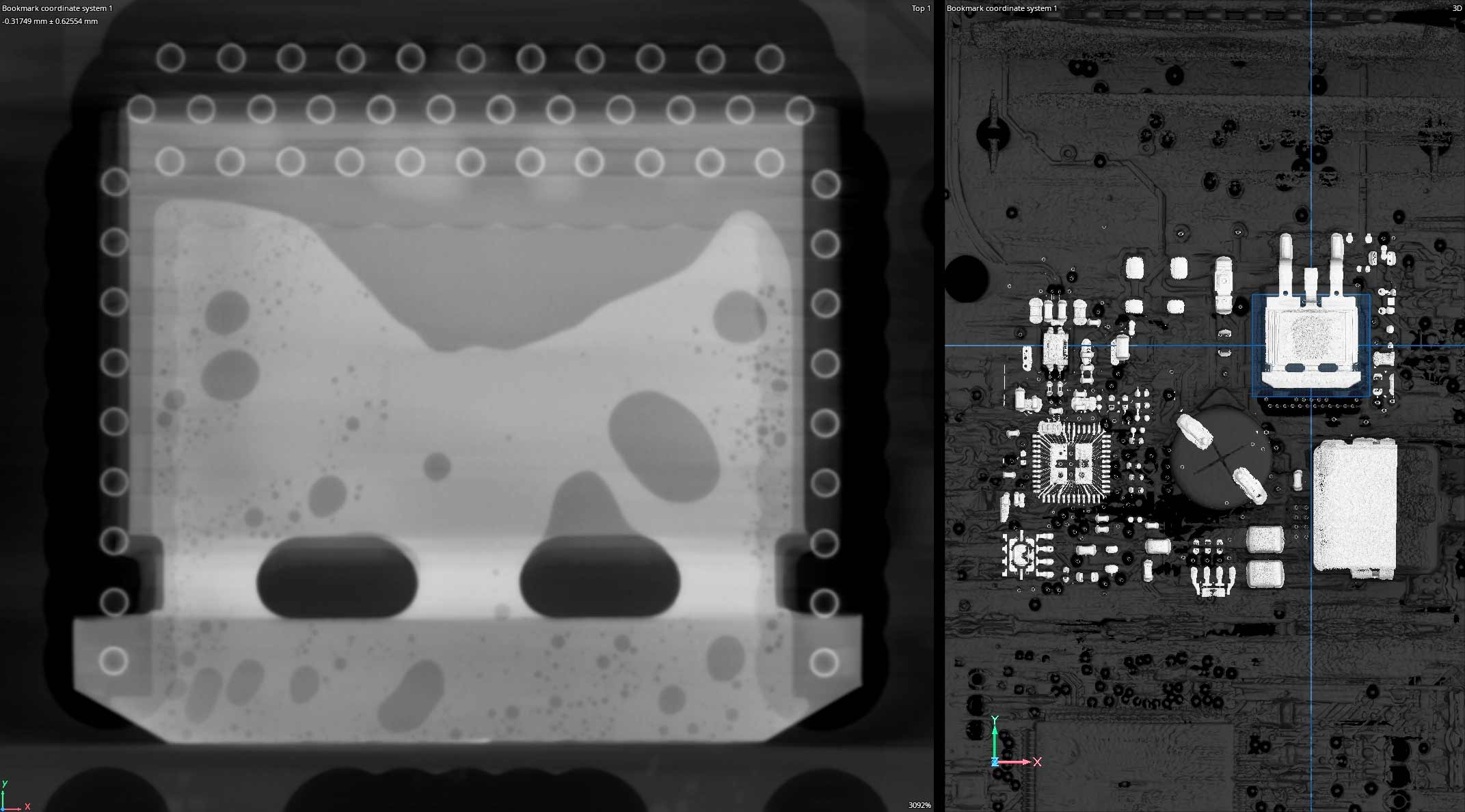
3D CT SCANNING
3D CT scanning offers an additional viewing axis for inspection. With 2D X-Ray all geometry in the view is viewed simultaneously. With 3D CT we can navigate through a tangible inspection volume where a larger variety of digital tools are available. For example, precise component alignments can be created. Additionally, dimensions can be extracted like depth of discontinuities, volumetric porosity, wall thickness, and complex 3D GD&T like flatness or feature positions.
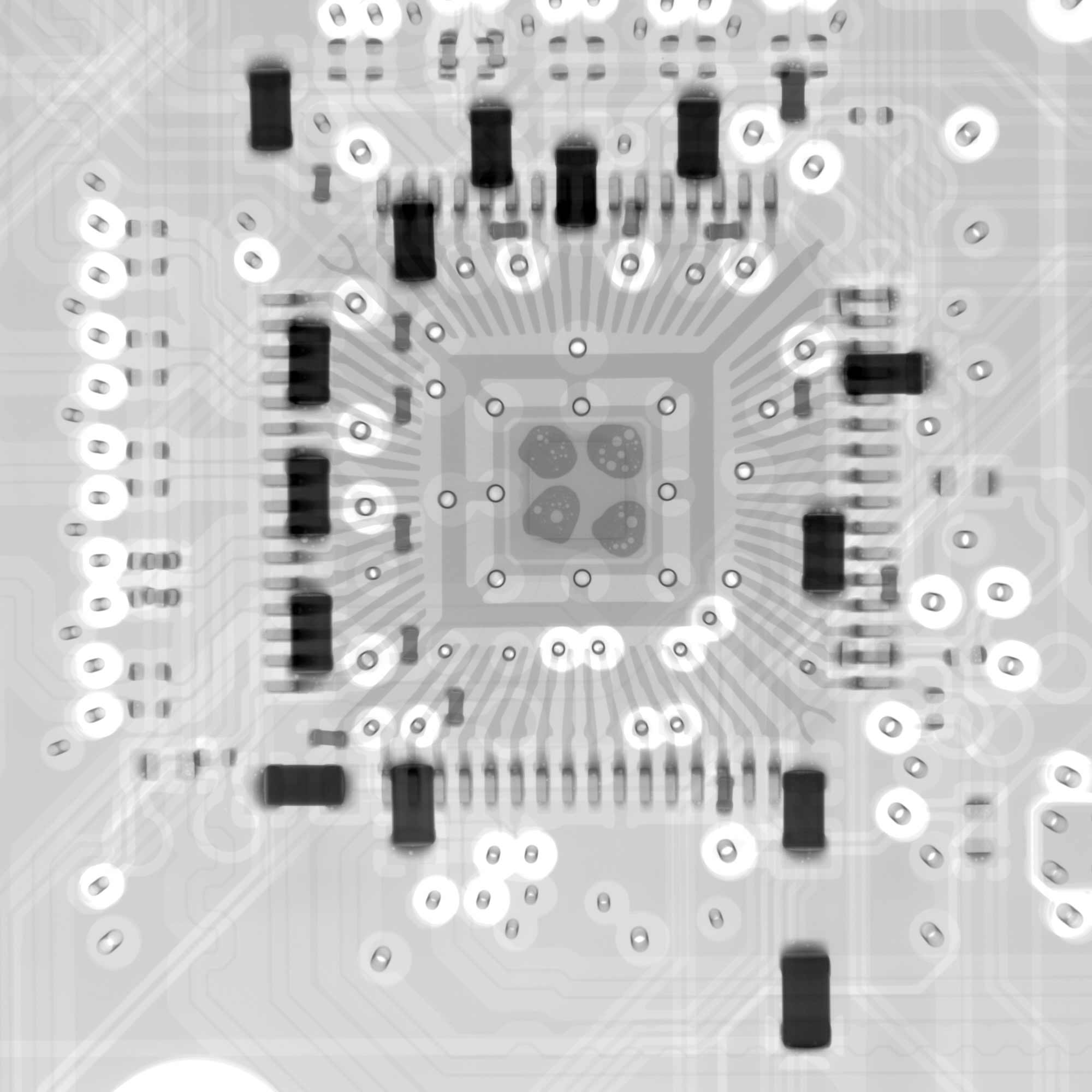
X-RAY IMAGING
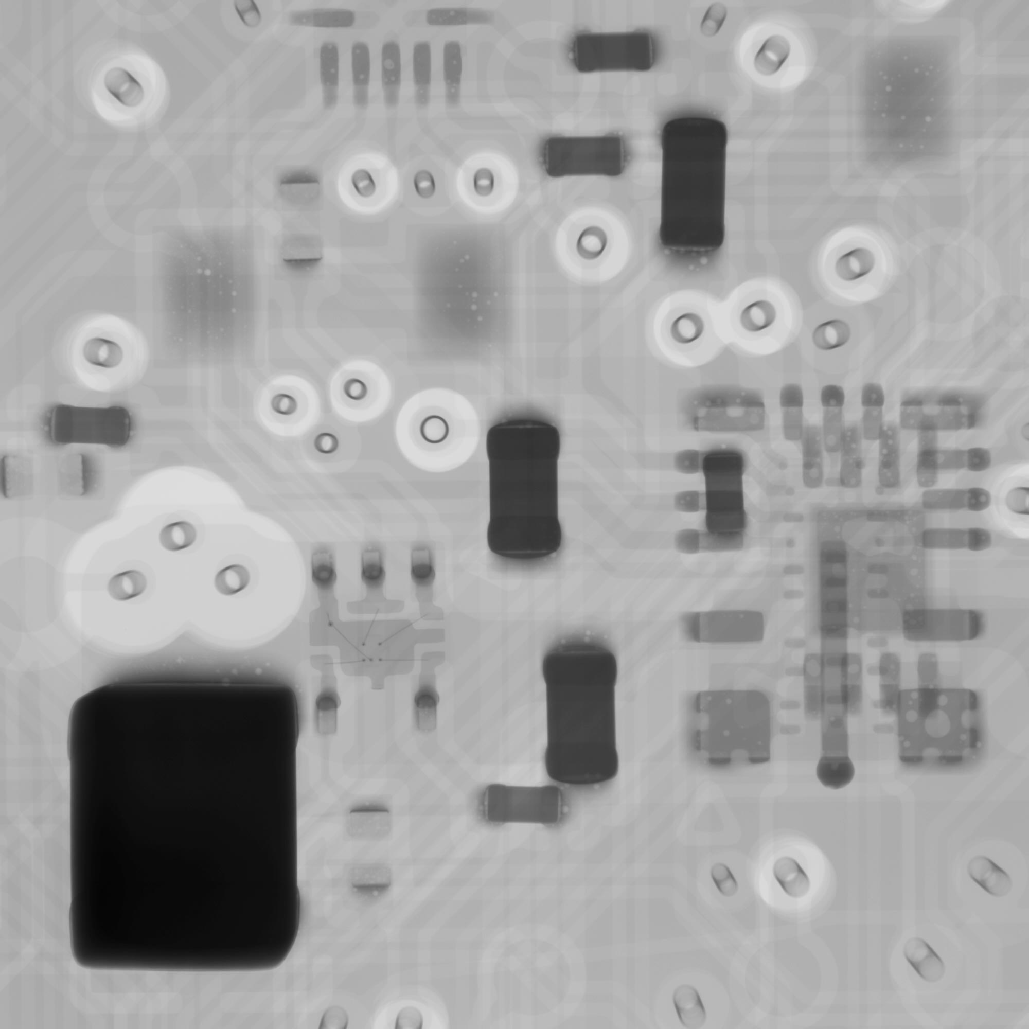
CT IMAGING
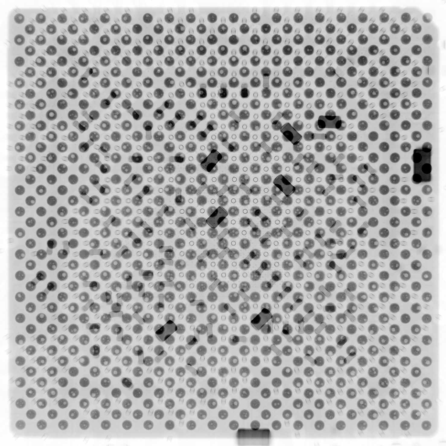
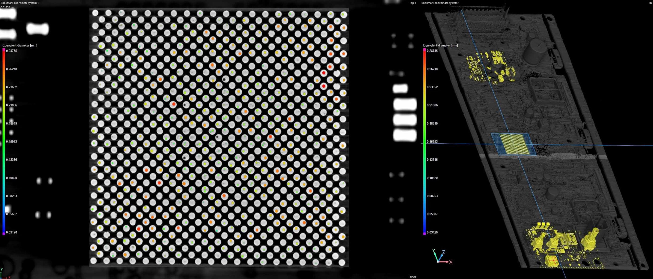
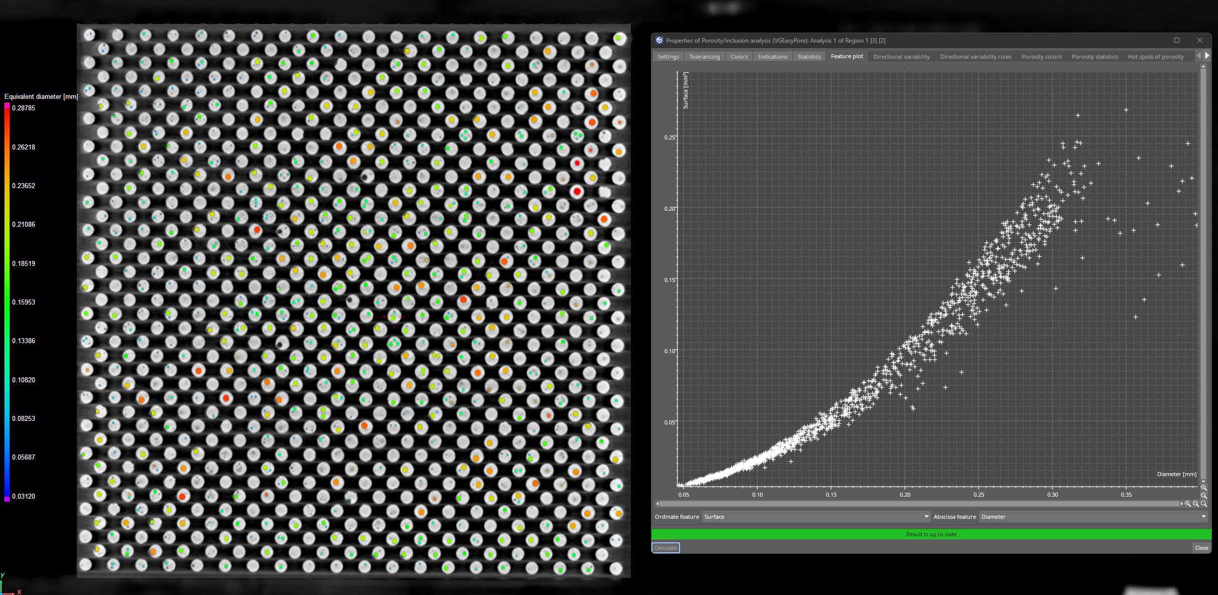
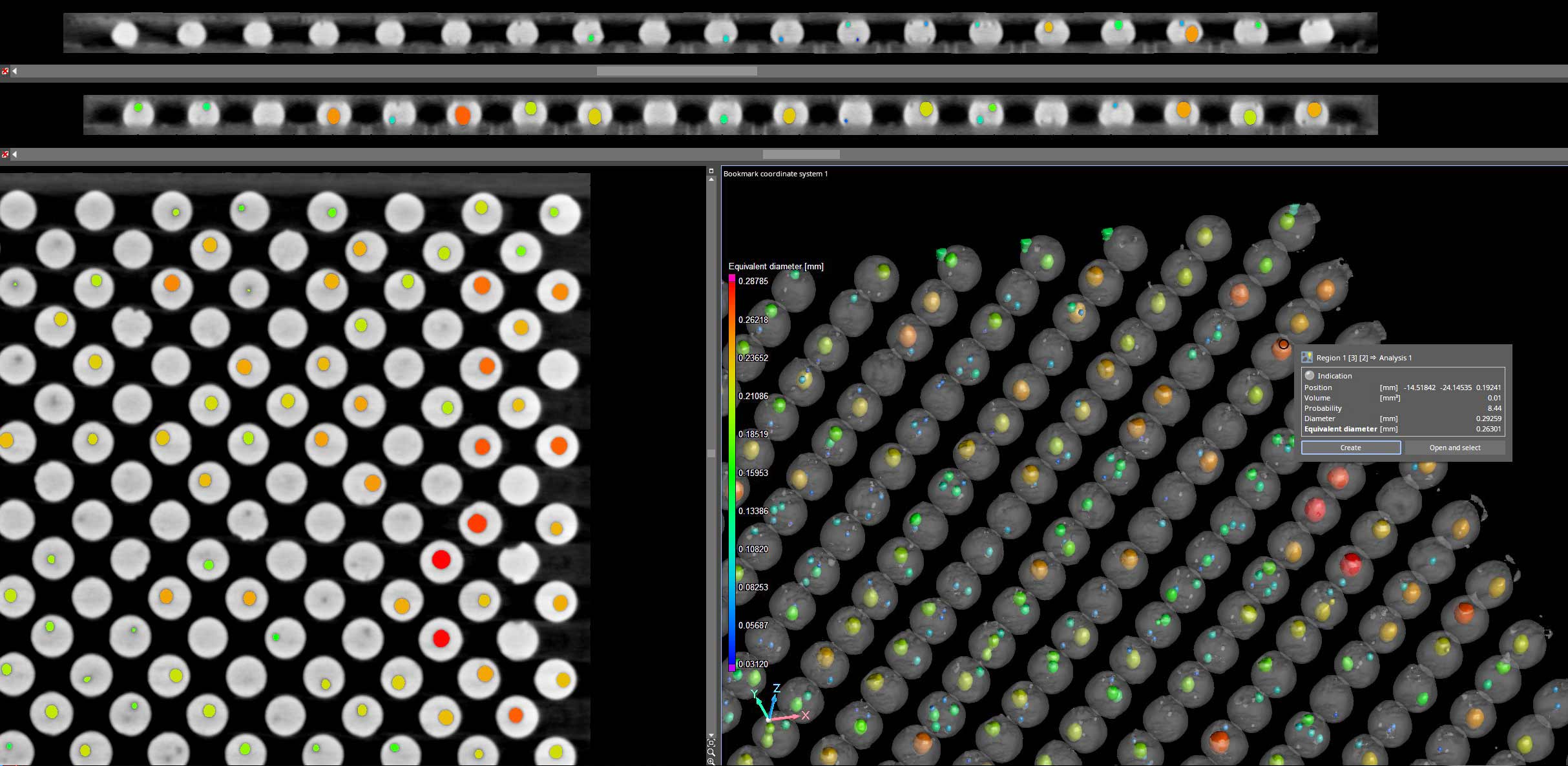
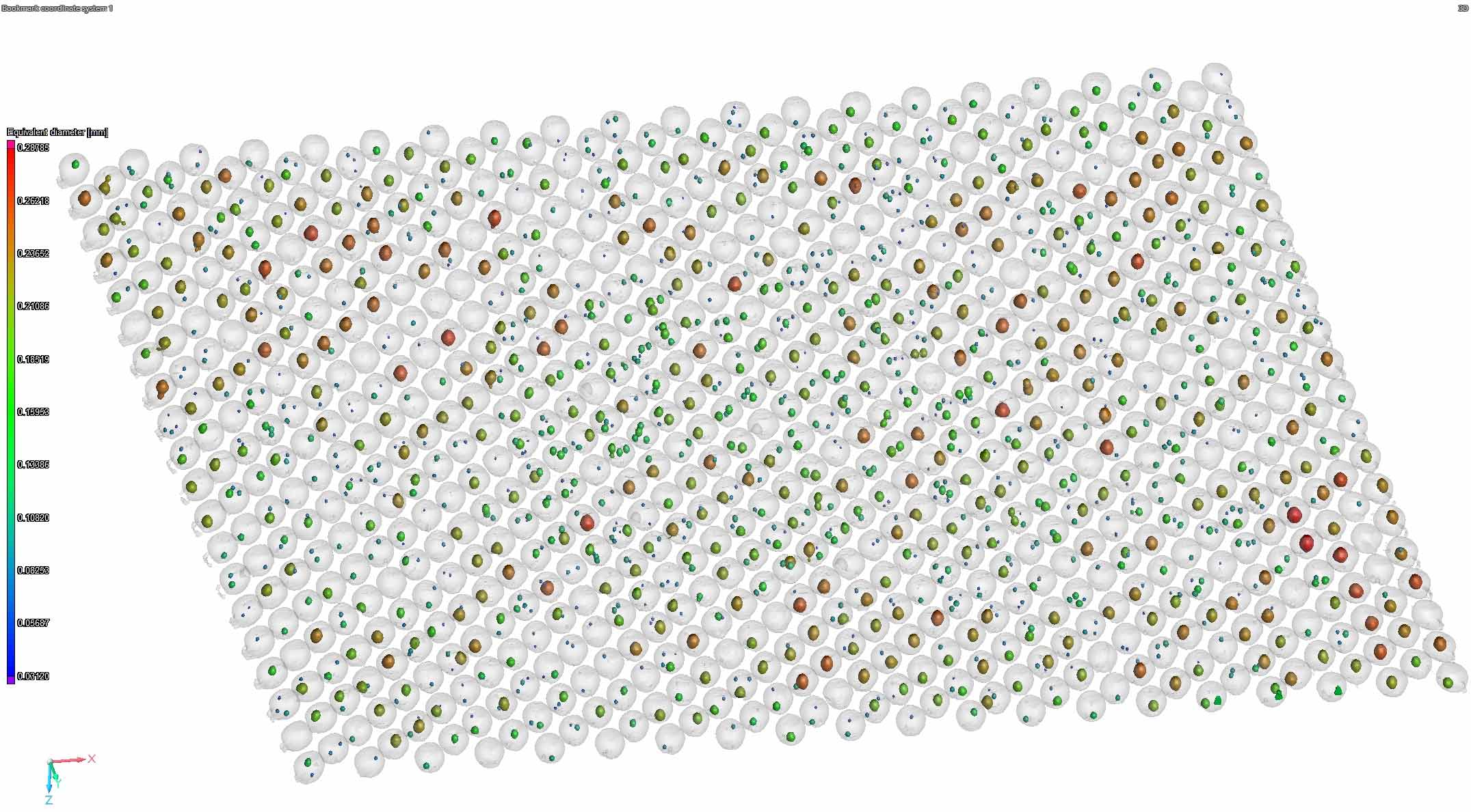
VOLUMETRIC POROSITY & DATA EVALUATION
Porosity can be extracted, volumetrically quantified, and exported into Excel. Such values as total porosity percentage, individual pore volume, equivalent diameter, and XYZ positional data can be produced.
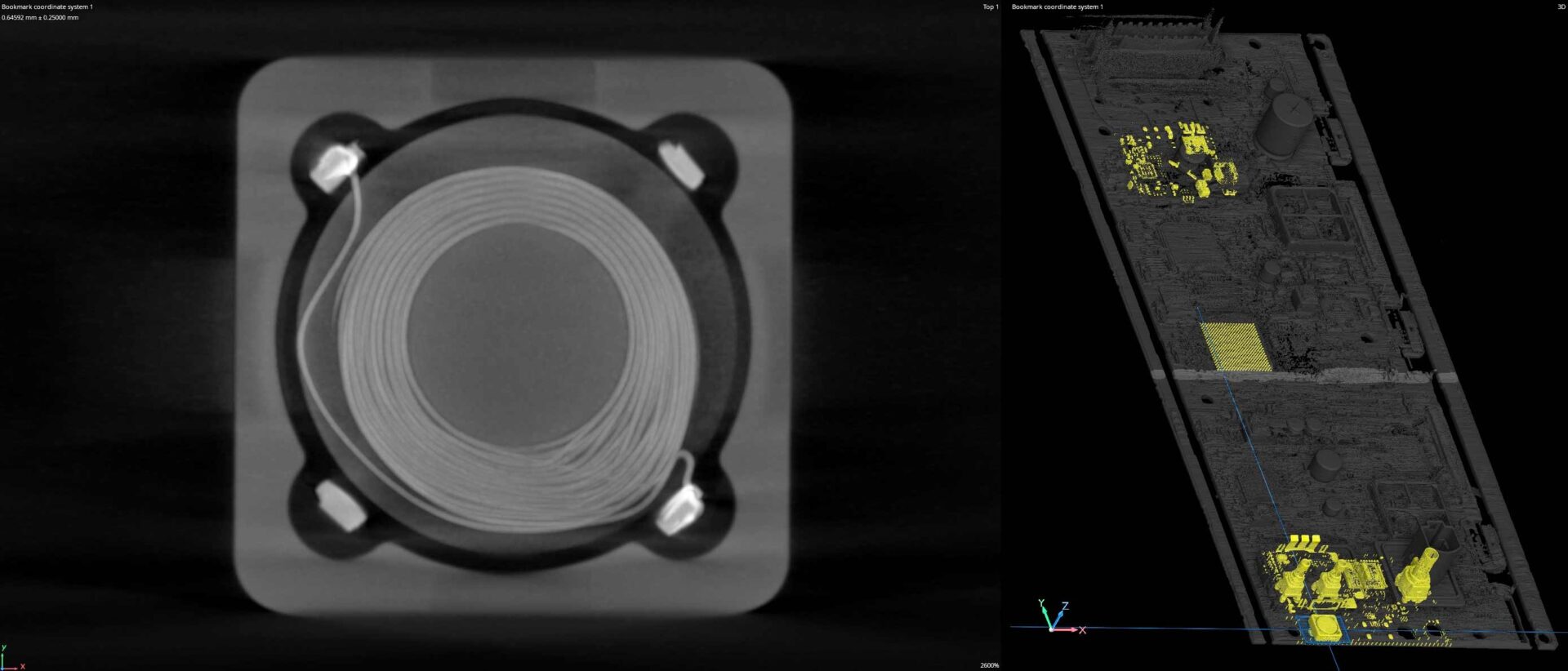
VIEWING FILTERS
Various viewing filters can be applied to the CT slice data. Instead of looking through a single slice of geometry, we can look at the highest density features across a specified length. For example, the bond wires below are imaged using a maximum density filter across a 2mm zone. If data is particularly noisy, an average min/max filter can be applied to help the inspector understand the geometry.