DIGITAL X-RAY INSPECTION OF PCBs
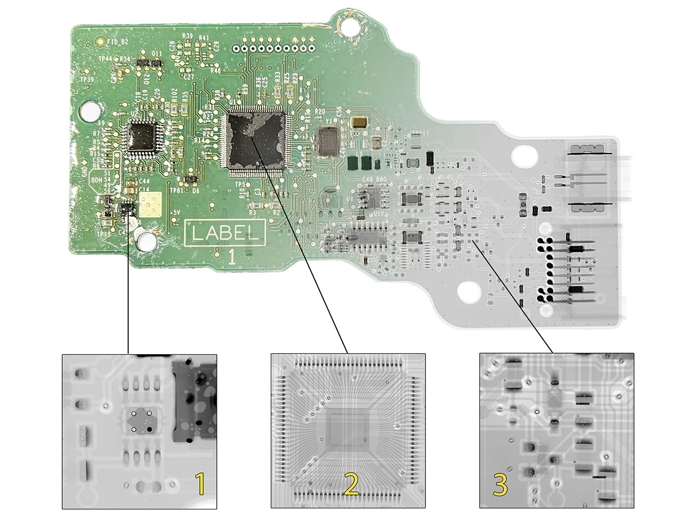
X-ray inspection is used to inspect the quality and reliability of products containing electronics by revealing hidden defects such as soldering issues, voids, misalignments, and component damage that may not be visible externally. By identifying potential problems early in the production process, X-ray inspection helps prevent failures, reduce rework costs, and enhance the overall performance and longevity of these products. This post demonstrates three inspection tools made possible using high resolution digital x-ray imaging..
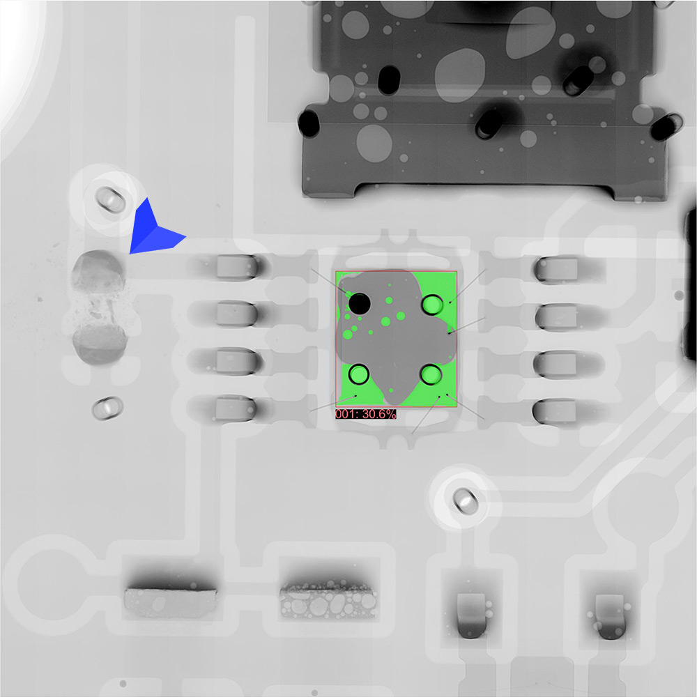
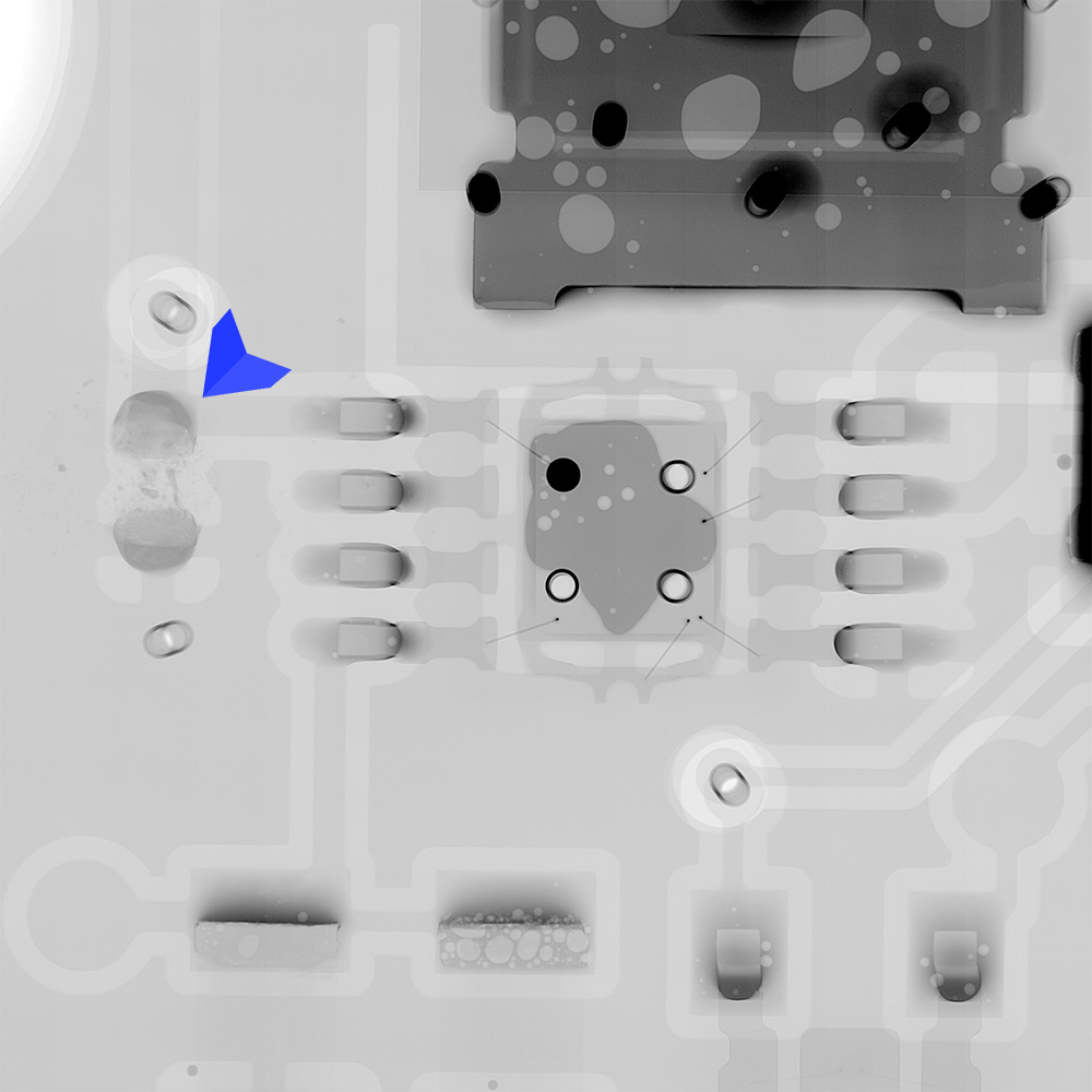
1. Solder Pad Fill
X-ray is used to ensure that the solder completely fills the pad to create a strong, conductive joint.
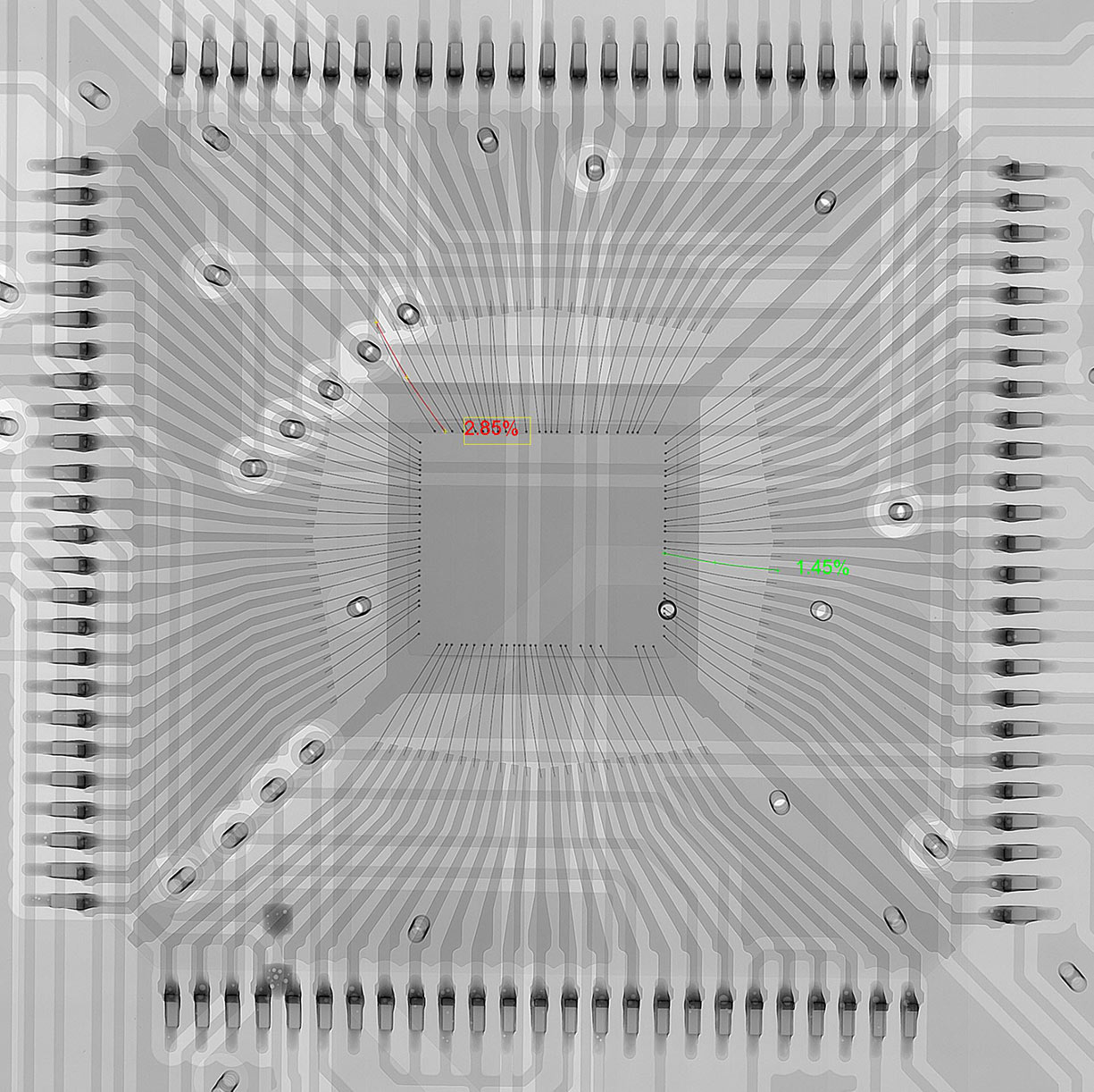
2. fpga wire sweep analysis
X-ray is used to examine the deformation of bonding wires within a microchip package which could potentially cause electrical shorts
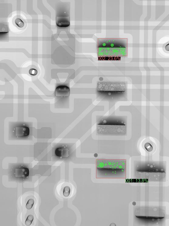
3. SOLDER JOINT POROSITY X-RAY INSPECTION
X-ray is used to detect small air pockets or voids within the solder joints of a printed circuit board. We follow custom quality standards provided by our clients to identify areas where process adjustments might be needed. For example, automotive porosity standards typically call for less than 20% porosity in any joint.
